Simple unch on transistors. Amplifier on transistors: species, schemes, simple and complex. Lamp sound amplifier
Low Frequency Amplifiers (UNG) are used to convert weak signals of predominantly audio range into more powerful signals, acceptable for direct perception through electrodynamic or other sound emitters.
Note that high-frequency amplifiers to frequencies 10 ... 100 MHz are built by similar schemes, all differences are most often reduced to the fact that the capacitors of the capacitors of such amplifiers decrease into as many times as the frequency of the high frequency signal exceeds the low-frequency frequency.
Simple amplifier on one transistor
The simplest UHF, made according to the scheme with a common emitter, is shown in Fig. 1. As a load used telephone caps. Permissible supply voltage for this amplifier 3 ... 12 V.
The value of the displacement resistor R1 (tens of kΩ) is desirable to determine experimentally, since its optimal value depends on the supply voltage of the amplifier, resistance of the telephone caps, the transmission coefficient of a specific transistor instance.
Fig. 1. Scheme of a simple UNG on one transistor + condenser and resistor.
To select the initial value of the resistor R1, it should be noted that its value is approximately a hundred and more times should exceed the resistance included in the load circuit. To select the displacement resistor, it is recommended to sequentially enable a constant resistor with a resistance of 20 ... 30 kΩ and a variable resistance of 100 ... 1000 com, after which, having feeding a small amplitude beep to the amplifier input, for example, from a tape recorder or player, rotating the variable resistor handle to achieve The best signal quality with its highest volume.
The capacity of the C1 transition capacitor (Fig. 1) may be between 1 to 100 microfosters: the greater the value of this container, the lower the low frequencies can increase UH. To master the low-frequency gain techniques, it is recommended to experiment with the selection of the items and modes of the amplifiers (Fig. 1 - 4).
Improvement options for one-window amplifier
Compared and improved compared to the scheme in Fig. 1 amplifier circuits are shown in Fig. 2 and 3. In the scheme in Fig. 2 The amplification cascade further comprises a frequency-dependent negative feedback chain (R2 resistor and C2 condenser), which improves the quality of the signal.
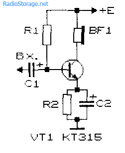
Fig. 2. Scheme of one-window UHC with a chain of a frequency-dependent negative feedback.
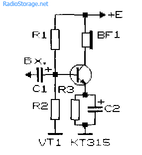
Fig. 3. One-window amplifier with a divider for feeding the bias voltage to the transistor base.

Fig. 4. One-window amplifier with automatic displacement setting for the transistor base.
In the diagram in fig. 3 The displacement to the transistor database is set to more "rigid" using a divider, which improves the quality of the amplifier when the conditions change its operation. "Automatic" installation of offset on the basis of the amplifying transistor is applied in the diagram in Fig. four.
Double-stage amplifier on transistors
By connecting sequentially two simple gain cascades (Fig. 1), you can get a two-stage UH (Fig. 5). Strengthening such an amplifier is equal to the product of the gain of separately taken cascades. However, it is not easy to get a large steady gain with the subsequent buildup of the number of cascades: the amplifier is likely to self-prompt.
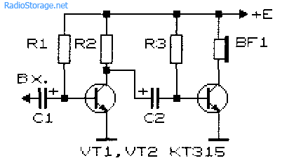
Fig. 5. Scheme of a simple two-stage wheel amplifier.
New developments of LF amplifiers, the schemes of which are often leading on the pages of the magazines of recent years, one is pursued by the goal of achieving the minimum coefficient of nonlinear distortion, increasing the output power, expansion of the frequency strengthened, etc.
At the same time, when setting up various devices and conducting experiments, a simple UNG is often needed, which can be collected in a few minutes. This amplifier must contain a minimum number of scarce elements and work in a wide range of supply voltage and load resistance.
Uncle scheme on wild and silicon transistors
The scheme of a simple power amplifier with a direct connection between the cascades is shown in Fig. 6 [РЛ 3 / 00-14]. The input impedance of the amplifier is determined by the ratiomiometer R1 ratio and can vary from hundreds of Ohm to dozen. At the output of the amplifier, you can connect the load with resistance from 2 ... 4 to 64 ohms and above.
With high-resistant load, the KT315 transistor can be used as VT2. The amplifier is operational in the range of supply voltages from 3 to 15 V, although its acceptable performance is maintained and with a decrease in supply voltage up to 0.6 V.
Capacitance C1 capacitor can be selected from 1 to 100 μF. In the latter case (C1 \u003d 100 μF) UUH can operate in the frequency band from 50 Hz to 200 kHz and above.

Fig. 6. Scheme of a simple low frequency amplifier on two transistors.
The amplitude of the ONLC input signal should not exceed 0.5 ... 0.7 V. The output power of the amplifier may vary from tens of MW to units of W, depending on the load resistance and the supply voltage.
The amplifier setting is the selection of resistors R2 and R3. With their help, the voltage on the transistor VT1 transistor, equal to 50 ... 60% of the power supply voltage. The VT2 transistor must be installed on the heat sink plate (radiator).
Tracked UNUC with direct connection
In fig. 7 shows a diagram of another externally simple UNG with direct connections between the cascades. This kind of communication improves the frequency characteristics of the amplifier in the lower frequency region, the scheme is generally simplified.
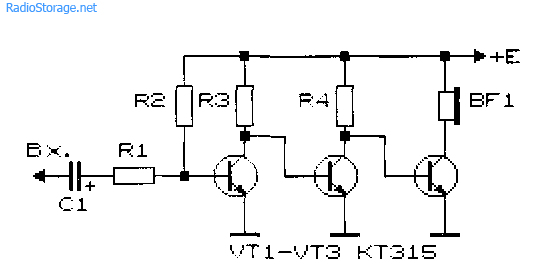
Fig. 7. Schematic diagram of a three-stage UHN with a direct connection between the cascades.
At the same time, the amplifier setting is complicated by the fact that each resistance of the amplifier has to be chosen individually. Approximately the ratio of resistors R2 and R3, R3 and R4, R4 and R BF should be within (30 ... 50) to 1. The resistor R1 must be 0.1 ... 2 com. Calculation of the amplifier shown in Fig. 7, it can be found in the literature, for example, [p 9 / 70-60].
Schemes of cascade unch on bipolar transistors
In fig. 8 and 9 show cascading unch schemes on bipolar transistors. Such amplifiers have a rather high gain coefficient. Amplifier in fig. 8 has ku \u003d 5 in the frequency band from 30 Hz to 120 kHz [MK 2/86-15]. Unch according to the scheme in fig. 9 With the harmonic coefficient, less than 1% has a gain 100 [RL 3 / 99-10].

Fig. 8. Cascade UMLC on two transistors with gain ratio \u003d 5.

Fig. 9. Cascade Ugra on two transistors with gain ratio \u003d 100.
Economical UMLC on three transistors
For portable radio electronic equipment, an important parameter is the cost effectiveness of UNG. The scheme of such a UHC is presented in Fig. 10 [RL 3 / 00-14]. Here used cascade inclusion of the VT1 field transistor and the bipolar transistor VT3, and the VT2 transistor is turned on in such a way that it stabilizes the operating point VT1 and VT3.
With an increase in the input voltage, this transistor shunt the emitter transition is the base VT3 and reduces the value of the current flowing through the transistors VT1 and VT3.

Fig. 10. Scheme of a simple economical LF amplifier on three transistors.
As in the above scheme (see Fig. 6), the input resistance of this UNch can be set from tens of dozen. A telephone capsession is used as a load, for example, TK-67 or TM-2B. A telephone capal, connected using a plug, can simultaneously serve as a power switch circuit.
The power supply voltage is from 1.5 to 15 V, although the performance of the device is maintained and with a decrease in the supply voltage to 0.6 V. in the 2 ... 15 supply voltage range, the current consumed by the amplifier is described by the expression:
1 (MCA) \u003d 52 + 13 * (Upit) * (Upit),
wHERE UPIT - Voltage voltage (B).
If you turn off the VT2 transistor, the current consumed by the current increases by an order.
Two-stage unch with direct connection between cascades
Examples of unch with direct connections and the minimum selection of operation mode are the schemes shown in Fig. 11 - 14. They have a high gain ratio and good stability.

Fig. 11. Simple dual-stage UHC for microphone (low noise level, high ku).

Fig. 12. Double low frequency amplifier on KT315 transistors.
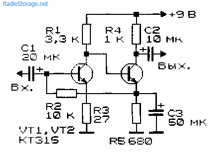
Fig. 13. Double low-frequency amplifier on KT315 transistors - option 2.
The microphone amplifier (Fig. 11) is characterized by a low level of own noise and a high gain [MK 5/83-XIV]. An electrodynamic type microphone is used as a microphone.
The role of a microphone can be a telephone caps. Stabilization of the working point (initial offset based on the input transistor) amplifiers in Fig. 11 - 13 is carried out due to the voltage drop on the emitter resistance of the second cascade of amplification.
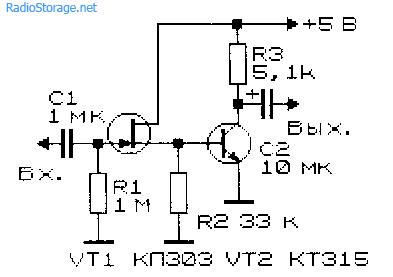
Fig. 14. Two-stage unch with a field transistor.
The amplifier (Fig. 14), having a high input impedance (of the order of 1 MΩ), is made on the field transistor VT1 (the founder) and bipolar - VT2 (with shared).
Cascade low-frequency amplifier on field transistors, also having a high input resistance, is shown in Fig. fifteen.

Fig. 15. Scheme of a simple two-stage unch on two field transistors.
Uncle Schemes for Low Residue
Typical UHCs designed to work on the low-voltage load and having the output power of dozens of MW and above, depicted in Fig. 16, 17.

Fig. 16. Simple UNG for working with low-resistance load.
The WAP electrodynamic head can be connected to the output of the amplifier, as shown in Fig. 16, either in the diagonal of the bridge (Fig. 17). If the power source is made of two consecutively connected batteries (batteries), the right-hand output of the VAP head can be connected to their middle point directly, without SZ capacitors, C4.
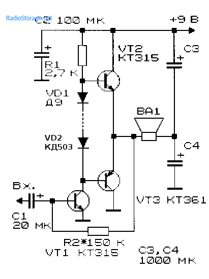
Fig. 17. Low frequency amplifier circuit with low-voltage load in the bridge diagonal.
If you need a simple lamp ungent scheme, then such an amplifier can be collected even on a single lamp, look at our electronics website in the appropriate section.
Literature: Shustov MA Practical scheme engineering (book 1), 2003.
Corrections in Publications: In fig. 16 and 17 instead of diode D9 installed a chain of diodes.
Transistor amplifiers, despite the appearance of more modern microcircuits, did not lose their relevance. It sometimes happens to get a microcircuit, sometimes it is not so easy, but the transistors can be dropped from almost any electronic device, which is why the mountains of these parts sometimes accumulate in avid radio amateurs. In order to find an application that suggests an imperial transistive power amplifier to the assembly, the assembly of which will be aspid even a beginner.
Scheme
The scheme consists of 6 transistors and can develop power up to 3 watts when powering with a voltage of 12 volts. This power is enough to voicing a small room or workplace. T5 and T6 transistors in the diagram form output cascade, in their place you can put widespread domestic analogues of KT814 and KT815. The C4 condenser, which connects to the output transistor collectors, separates the constant component of the output signal, which is why this amplifier can be used without the protection of acoustic systems. Even if the amplifier in the process fails and constant voltage will appear at the output, it will not be on the condenser and the speakers of the speaker system will remain well. The separator capacitor C1 at the entrance is better to apply the film, but if it is not at hand, it will come up and ceramic. The analogue of D1 and D2 diodes in this scheme is 1N4007 or domestic KD522. The speaker can be used with a resistance of 4-16 ohms, the lower resistance, the greater power will develop the scheme.(Dropping: 686)

Assembling amplifier
A scheme is collected on a circuit board with dimensions of 50x40 mm, the picture in the Sprint-layout format is attached to the article. The given printed circuit board must be selected. After etching and removing the toner from the board, the holes are drilled, it is best to use the drill 0.8 - 1 mm, and for holes under the output transistors and a terminal bar of 1.2 mm.
After drilling holes, it is advisable to raid all the tracks, thereby reducing their resistance and protect copper from oxidation. Then minor parts are soldered - resistors, diodes, after which the weekend transistors, terminal bar, capacitors. According to the scheme, the output transistors should be connected, on this board, this compound occurs by closing the "backs" of transistors with wire or radiator if used. The radiator is required to be installed if the diagram is loaded on the speaker 4 ohm resistance, or if the high volume signal is gave to the input. In the remaining cases, the output transistors are almost not heated and do not require additional cooling.

After the assembly, it is necessary to wash off the flux residues from the tracks, check the fee for assembling errors or closures between adjacent tracks.
Adjusting and testing amplifier
After the assembly is completed, you can apply power to the amplifier fee. In the gap of one of the feed wires, you need to turn on the ammeter to control the current consumption. Let's supply power and look at the ammeter readings, the amplifier must consume approximately 15-20 mA without feeding the signal. The rest current is set by the R6 resistor, to increase it, it is necessary to reduce the resistance of this resistor. Too much of the rest of the rest should not, because The heat release in the output transistors will increase. If the rest is normal, you can feed the signal to the input, for example, music from a computer, phone or player, connect the speaker to the output and start listening. Although the amplifier is simple, it provides very acceptable sound quality. To play both two channels, left and right, the diagram must be collected twice. Please note that if the signal source is far from the board, it is necessary to connect it to the shielded wire, otherwise it does not avoid interference and tip. Thus, this amplifier turned out to be fully universal due to low current consumption and compact fees. It can be used both as part of computer columns and when creating a small stationary music center. Successful assembly. Good afternoon, a respected Hamburazer, I want to tell you about the basics of building sound frequency amplifiers. I think this article will be interested in you if you have never been engaged in electronics, and of course it will be ridiculous to those who do not part with the soldering iron. And so I will try to tell about this topic as simple as possible and unfortunately lowering some nuances.Sound frequency amplifier or low frequency amplifier to figure out how it all works and why there are so many any transistors, resistors and capacitors, you need to understand how each element works and try to learn how these elements are arranged. In order to assemble a primitive amplifier, we will need three types of electronic elements: resistors, condensers and of course transistors.
Resistor
So, the resistors are characterized by electrical current resistance and this resistance is measured in Oma. Each electrically conductive metal or metal alloy has its own resistivity. If we take the wire defined long with high resistivity, then we will have a real wire resistor. In order for the resistor to be compact, wire can be coated on the frame. Thus, we will have a wire resistor, but it has a number of disadvantages, therefore resistors are usually made from metal-ceramic material. This is how the resistors on the electrical circuits are indicated:The top version is adopted in the United States, the lower in Russia and in Europe.
Capacitor
The condenser is two metal plates separated by dielectric. If we give constant voltage on these plates, the electrical field will appear, which, after turning off the power, will support positive and negative charges on the plates, respectively.
The basis of the condenser design - two conductive plates, between which the dielectric is located
Thus, the capacitor is able to accumulate an electric charge. This ability to accumulate electrical charge is called the electrical capacity that is the main parameter of the condenser. Electrical container is measured in the Farades. What is still characteristic, this is what when we charge or discharge the capacitor, an electric current is going through it. But as soon as the capacitor charged, he ceases to skip the electric current, and this is because the capacitor accepted the power supply charge, that is, the potential of the capacitor and the power source is the same, and if there is no potential difference (voltage), no electric current. Thus, the charged capacitor does not skip the constant electric current, but passes an alternating current, since when it is connected to a variable electric current, it will be constantly charged and discharged. On electrical circuits, it is denoted:

Transistor
In our amplifier, we will use the simplest bipolar transistors. The transistor is made from semiconductor material. The property necessary for us is a material - the presence of free media in them both positive and negative charges. Depending on which charges are more, semiconductors are distinguished by two types of conductivity: n.-Type I. p.-Type (N-Negative, P-Positive). Negative charges are electrons released from the outer shells of the atoms of the crystal lattice, and positive - so-called holes. The holes are vacant places that remain in electronic shells after leaving electrons. Conventionally denotes atoms with an electron on an external orbit with a blue circle with a minus sign, and atoms with a vacant place - an empty mug:
Each bipolar transistor consists of three zones of such semiconductors, these zones call the base, emitter and collector.

Consider an example of the transistor. To do this, connect to the transistor two batteries by 1.5 and 5 volts, plus to the issuer, and a minus to the database and collector, respectively (see figure):

On the contact of the base and emitter, an electromagnetic field will appear, which literally cuts electrons from the external orbit of the base atoms and transfers them to the emitter. Free electrons leave holes behind them, and occupy vacant places already in Emitter. The same electromagnetic field has the same effect on the collector atoms, and since the base in the transistor is quite thin relative to the emitter and manifold, the collector's electrons are quite easy to pass through it into the emitter, and in much more quantity than from the base.
If we turn off the voltage from the base, then there will be no electromagnetic field, and the base will perform the role of a dielectric, and the transistor will be closed. Thus, when applying a small voltage to the base, we can control the larger tension to the emitter and the collector.
Transistor considered by us pNP.-Type, since he has two p.- And alone n.-zone. Also exist nPN.-Transistors, the principle of operation in them is the same, but the electric current flows in them in the opposite direction than in the transistor considered by us. So bipolar transistors are indicated on electrical circuits, the arrow indicates the current direction: 
UNG
Well, let's try to design a low frequency amplifier from this. First, we need a signal that we will strengthen, it can be a sound card of a computer or any other sound device with a linear output. Suppose our signal with a maximum amplitude of about 0.5 volts at a current of 0.2 A, approximately such:
And what would earn the simplest 4 ohm 10 watt speaker, we need to increase the amplitude of the signal to 6 volts, with current strength I. = U. / R. \u003d 6/4 \u003d 1.5 A.
So, let's try to connect our signal to the transistor. Remember our transistor and two batteries, now instead of a 1.5 volt battery, we have a linear output signal. The R1 resistor performs the role of the load, in order not there was a short circuit and our transistor has not burned down.

But here there are two problems at once, first our transistor nPN.-Type, and opens only with a positive value of the half-wave, and when negative is closed.

Secondly, the transistor, as well as any semiconductor device, has nonlinear characteristics regarding voltage and current and the smaller the current and voltage values \u200b\u200bare the stronger these distortion:

Not only from our signal remained only half-wave, so it will also be distorted:

This is the so-called stitch type distortion.
To get rid of these problems, we need to shift our signal to the transistor working area, where the entire signal sinusoid and nonlinear distortions will be insignificant. For this, the bias voltage is fed to the base, allowing 1 volts, using a voltage divider and R3 composed of two resistors.

And our signal entering the transistor will look like this:

Now we need to withdraw our useful signal from the collector of the transistor. To do this, set the C1 condenser:

As we remember the capacitor skips alternating current and does not miss a permanent, so it will serve as a filter only our useful signal - our sinusoid. And the constant component that did not pass through the capacitor will dissipate on the R1 resistor. The alternating current, our useful signal, will strive to go through the condenser, so the resistance of the capacitor for it is negligible compared to the R1 resistor.
So it turned out the first transistor cascade of our amplifier. But there are two more small nuances:
We do not know 100% which signal is included in the amplifier, suddenly all the same source of the signal is faulty, anything happens, again static electricity or with a useful signal passes a constant voltage. This may cause not the correct operation of the transistor or even provoke its breakdown. To do this, we will establish C2 capacitor, it is similar to C1 condenser will block a constant electric current, as well as the limited capacitance of the capacitor will not pass the peaks of large amplitudes that can spoil the transistor. Such voltage jumps usually occur when the device is turned on or disconnected.

Both the second nuance, any source of the signal, a certain particular load is required (resistance). Therefore, the input resistance of the cascade is important for us. To adjust the input resistance, add the R4 resistor to the Emitter chain:

Now we know the appointment of each resistor and the condenser in the transistor cascade. Let's now try to calculate what nominal items need to be used for it.
Initial data:
- U. \u003d 12 V - supply voltage;
- U BE ~ 1 V - voltage emitter-base of the operating point of the transistor;

- P Max \u003d 200 MW - maximum power dissipation;
- I Max \u003d 100 mA - maximum direct current collector;
- U Max \u003d 18 V - Maximum permissible voltage collector-base / collector-emitter (we have a supply voltage of 12 V, so it is enough with a margin);
- U Eb. \u003d 5 V - Maximum allowable voltage emitter base (our voltage 1 volt ± 0.5 volt);
- h21 \u003d 75-225 - the reducing coefficient of the base current, the minimum value is taken - 75;
- We calculate the maximum static power of the transistor, it takes it by 20% less than the maximum power dissipated, in order to do our transistor did not work at the limit of its capabilities:
P Art.max = 0,8*P Max \u003d 0.8 * 200 mW \u003d 160 MW;
- We define the collector current in the static mode (without a signal), despite the fact that the voltage is not supplied through the transistor anyway, the electric current flows into a low.
I K0. = P Art.max / U CEwhere U CE - Transition voltage collector-emitter. On the transistor, half of the supply voltage is scattered, the second half will dissipate on the resistors:
U CE = U. / 2;
I K0. = P Art.max / (U. / 2) \u003d 160 MW / (12V / 2) \u003d 26.7 MA;
- Now we calculate the load resistance, initially we had one resistor R1, which performed this role, but since we have added a R4 resistor to increase the input resistance of the cascade, now the load resistance will be folded from R1 and R4:
R N. = R1 + R4.where R N. - general load resistance;
The ratio between R1 and R4 is usually taken 1 to 10:
R1 = R4.*10;
Calculate the load resistance:
R1 + R4. = (U. / 2) / I K0. \u003d (12V / 2) / 26.7 Ma \u003d (12V / 2) / 0.0267 A \u003d 224.7 Ohm;
The coming quantor rates are 200 and 27 ohms. R1 \u003d 200 ohm, and R4. \u003d 27 ohms.
- Now we find the voltage on the transistor collector without a signal:
U K0. = (U CE0. + I K0. * R4.) = (U. - I K0. * R1) \u003d (12V -0.0267 A * 200 Ohm) \u003d 6.7 V;
- The current of the transistor control database:
I B. = I K. / h21where I K. - collector current;
I K. = (U. / R N.);
I B. = (U. / R N.) / h21 \u003d (12V / (200 Ohm + 27 Ohm)) / 75 \u003d 0.0007 A \u003d 0.07 MA;
- The full current of the base is determined by the bias voltage on the base, which is set by the divider R2 and R3. The current specifier must be 5-10 times the base current of the base ( I B.) What actually actually does not affect the offset voltage. Thus, for the value of the divider current ( I Affairs) Take 0.7 MA and expect R2 and R3:
R2 + R3 = U. / I Affairs \u003d 12V / 0.007 \u003d 1714.3 Ohm
- Now we calculate the voltage on the emitter at rest of the transistor ( U E.):
U E. = I K0. * R4. \u003d 0.0267 A * 27 Ohm \u003d 0.72 V
Yes, I K0. a reservoir resting current, but the same current passes through the emitter, so I K0. They consider the rest of the entire transistor.
- Calculate the full voltage based on the database ( U B.) taking into account the offset voltage ( U See \u003d 1B):
U B. = U E. + U See \u003d 0.72 + 1 \u003d 1.72 V
Now with the help of a voltage divider formula, we find the values \u200b\u200bof resistors R2 and R3:
R3 = (R2 + R3) * U B. / U. \u003d 1714.3 Ohm * 1.72 V / 12 V \u003d 245.7 ohms;
The nearest metal of the resistor is 250 ohms;
R2 = (R2 + R3) - R3 \u003d 1714.3 Ohm - 250 ohm \u003d 1464.3 Ohm;
The resistor's denomination is chosen towards the reduction, the nearest R2 \u003d 1.3 com.
- Condencators C1. and C2. Typically set at least 5 μF. Capacity is chosen such that the capacitor did not have time to recharge.
Conclusion
At the output of the cascade, we obtain a proportionally enhanced signal and for current and voltage, that is, by power. But we are not enough for one cascade for the required gain, so you have to add the following and next ... and so on.The considered calculation is rather superficial and such a gain scheme is of course not used in the structure of amplifiers, we should not forget about the range of frequencies of transmitted frequencies, distortions and many other things.
The simplest amplifier on transistors can be a good benefit to study the properties of the instruments. Schemes and designs are fairly simple, you can independently make the device and check it out, measure all parameters. Thanks to modern field transistors, you can make a miniature microphone amplifier literally from three elements. And connect it to a personal computer to improve recording parameters. Yes, and interlocutors in conversations will be much better and clearly heard your speech.
Frequency characteristics
Low (sound) frequency amplifiers are available in almost all household appliances - musical centers, televisions, radio receivers, radio tape recorders, and even in personal computers. But there are still RF amplifiers on transistors, lamps and chips. Their difference is that UNG allows the signal of only sound frequency, which is perceived by the human ear. Sound amplifiers on transistors allow you to play signals with frequencies in the range from 20 Hz to 20,000 Hz.
Consequently, even the simplest device can enhance the signal in this range. And it makes it as evenly uniform. The gain depends on the frequency of the input signal. The graph of the dependence of these values \u200b\u200bis a practically straight line. If you have a signal with a frequency outside the range, the quality of work and the efficiency of the device will quickly decrease. ONLC cascades are collected, as a rule, on transistors operating in low- and mid-frequency bands.
Sound amplifier work classes

All amplifying devices are divided into several classes, depending on which degree of flow during the current operation period through the cascade:
- The class "A" - the current proceeds to be non-stop during the entire period of the enhanced cascade.
- In the class of work "B" flows current within half of the period.
- The class "AB" suggests that the current flows through an amplifying cascade for a period of 50-100% of the period.
- In the "C" mode, the electric current leaks less than half the time of operation.
- The "D" mode of UNG is applied in amateur radio practice recently - a little over 50 years. In most cases, these devices are implemented on the basis of digital elements and have a very high efficiency - over 90%.
Availability of distortions in various classes of LF-amplifiers
The working area of \u200b\u200bthe transistor amplifier class "A" is characterized by quite small nonlinear distortions. If the incoming signal throws up a higher voltage pulses, this leads to the fact that the transistors are saturated. In the output signal, higher (up to 10 or 11) begin to appear near each harmonics. Because of this, a metallic sound appears, characteristic only for transistor amplifiers.
With unstable power, the output will be simulated by amplitude near the network frequency. The sound will be on the left side of the frequency response more rigid. But the better the stabilization of the power of the amplifier, the more difficult the design of the entire device becomes. UNG, working in the class "A", have a relatively small efficiency - less than 20%. The reason lies in the fact that the transistor is constantly open and the current through it constantly proceeds.

To increase (truth, minor) efficiency, you can use two-stroke schemes. One disadvantage - the half-wave of the output signal becomes asymmetrical. If we translate from the class "A" to "AB", nonlinear distortions will increase by 3-4 times. But the efficiency of the entire scheme of the device will still increase. UNUC classes "Av" and "B" characterizes the increase in distortion when the signal level is reduced at the input. But even if you add volume, it will not help completely get rid of flaws.
Work in intermediate classes
Each class has several varieties. For example, there is a class of work of amplifiers "A +". In it, transistors at the inlet (low-voltage) work in "A" mode. But high-voltage, installed in the output cascades, operate either in "B" or in "AB". Such amplifiers are much more economical than working in the class "A". A noticeably smaller number of non-linear distortions is not higher than 0.003%. You can achieve higher results using bipolar transistors. The principle of operation of amplifiers on these elements will be discussed below.
But still there is a large number of higher harmonics in the output signal, which is why the sound becomes characteristic of metallic. There are still amplifier schemes operating in AA class. They are non-linear distortions even less - to 0.0005%. But the main disadvantage of transistor amplifiers still has a characteristic metallic sound.
"Alternative" designs

It cannot be said that they are alternative, just some specialists engaged in designing and assembling amplifiers for high-quality sound reproduction, increasingly prefer the lamp structures. Lamp amplifiers have such advantages:
- Very low value of the level of nonlinear distortion in the output signal.
- Higher harmonics less than in transistor structures.
But there is one huge minus that outweighs all the advantages - it is necessary to put a device for coordination. The fact is that the lamp cascade has a lot of resistance - several thousand ohms. But the resistance of the speaker winding is 8 or 4 Ohm. To match them, you need to install a transformer.
Of course, this is not a very big drawback - there are transistor devices that use transformers to match the output cascade and an acoustic system. Some experts argue that the most effective scheme is a hybrid - which uses one-acting amplifiers that are not covered by negative feedback. Moreover, all these cascades are functioning in the UHC class "A" mode. In other words, it is used as a repeater power amplifier on a transistor.

Moreover, the efficiency of such devices are quite high - about 50%. But you should not focus only on efficiency and power indicators - they do not talk about high quality sound reproduction amplifier. The linearity of characteristics and their quality have much more important. Therefore, it is necessary to pay attention primarily on them, and not to power.
Scheme of one-stroke uncle on the transistor
The easiest amplifier, built according to the scheme with a common emitter, works in the class "A". The diagram uses a semiconductor element with the N-P-N structure. The collector chain is installed resistance R3, which limits the flowing current. The collector chain is connected to a positive power wire, and the emitter - with a negative one. In the case of using semiconductor transistors with the P-N-P structure, the scheme will be exactly the same, that's just a polarity will be changed.
Using the separation capacitor C1, it is possible to separate the variable input signal from the DC source. In this case, the capacitor is not an obstacle for the flow of AC along the path-emitter path. The internal resistance of the transition of the emitter base along with the resistors R1 and R2 is the simplest supply voltage divider. Usually, the R2 resistor has a resistance of 1-1.5 com - the most typical values \u200b\u200bfor such schemas. At the same time, the supply voltage is divided into exactly half. And if the voltage circuit is 20 volts, then you can see that the value of the gain coefficient in the current H21 will be 150. It should be noted that the AV amplifiers on the transistors are performed according to similar schemes, only work a little differently.

At the same time, the emitter voltage is 9 V and the fall on the section of the circuit "E - B" 0.7 V (which is typical for transistors on silicon crystals). If you consider an amplifier on Germany transistors, then in this case the voltage drop in the "E-b" section will be 0.3 V. The current in the collector circuit will be equal to the one that flows in the emitter. It is possible to calculate, dividing the emitter voltage to the resistance R2 - 9B / 1 com \u003d 9 mA. To calculate the value of the base current, it is necessary to divide 9 mA to the gain coefficient H21 - 9MA / 150 \u003d 60 μA. In the structures of UNG, bipolar transistors are usually used. The principle of operation is different from the field.
On the R1 resistor, you can now calculate the drop value - this is the difference between the database and power supply voltages. In this case, the base voltage can be found in the formula - the sum of the characteristics of the emitter and the transition "E-B". With diet from the source 20 volts: 20 - 9.7 \u003d 10.3. From here, you can calculate the resistance value R1 \u003d 10.3V / 60 μA \u003d 172 com. The C2 container is present in the diagram required to implement the circuit along which the emitter current component variable can be passed.
If you do not install C2 condenser, the variable component will be very limited. Because of this, such an amplifier of sound on the transistors will have a very low gain in terms of the current H21. It is necessary to draw attention to the fact that in the above calculations were taken equal toxes of the base and collector. And for the current, the base was taken by the one that flows into the chain from the emitter. It occurs only under the condition of feeding the bias voltage transistor base.

But it must be borne in mind that according to the circuit of the base is absolutely always, regardless of the presence of a displacement, the collector leakage current is necessarily flowing. In diagrams with a common emitter, the leakage current is intensified by no less than 150 times. But usually this value is taken into account only when calculating amplifiers on Germany transistors. In the case of using silicon, in which the current "K-b" circuit is very small, this value is simply neglected.
Amplifiers on TIR transistors
The amplifier on the field transistors, presented in the diagram, has many analogues. Including using bipolar transistors. Therefore, it can be considered as a similar example of a sound amplifier design assembled according to a circuit with a common emitter. The photo presents the scheme made according to the scheme with a common source. On the input and output circuits, R-C-communication is collected so that the device works in the AM amplifier mode.
A variable current from the signal source is separated from a constant supply voltage with a capacitor C1. Be sure to the amplifier on the field transistors must have a shutter potential, which will be lower than the similar source characteristic. On the presented scheme, the shutter is connected to the general wire by means of a resistor R1. Its resistance is very large - the resistors are usually used in the designs of 100-1000 com. Such a large resistance is chosen so that the input signal is not shunk.

This resistance almost does not pass the electric current, as a result of which the shutter has the potential (in the absence of a signal at the entrance) the same as the earth. At the source, the potential is higher than that of the Earth, only due to the voltage drop on the resistance R2. It is clear from here that the shutter has the potential lower than that of the source. Namely, this is required for the normal functioning of the transistor. It is necessary to pay attention to the fact that C2 and R3 in this amplifier scheme have the same purpose as in the design above. And the input signal is shifted relative to the outlet to 180 degrees.
Uncle with outlet transformer

You can make such an amplifier with your own hands for home use. It is performed according to the scheme operating in the class "A". The design is the same as discussed above, with a common emitter. One feature - you need to use a transformer to match. This is a disadvantage of such a sound amplifier on transistors.

The collector circuit of the transistor is loaded with the primary winding, which develops the output signal transmitted through the secondary speakers. On the resistors R1 and R3, the voltage divider is assembled, which allows you to select the operating point of the transistor. Using this chain, the bias voltage is supplied to the base. All other components have the same appointment as the schemes considered above.
Two-stroke audio amplifier
It is impossible to say that this is a simple amplifier on the transistors, since its work is a bit more complicated than those considered earlier. In the two-stroke unch, the input signal is split into two half-waves, various phases. And each of these half-filled with its cascade, made on the transistor. After the amplification of each half-wave occurred, both signals are connected and arrived on the speakers. Such complex transformations are able to cause signal distortions, since the dynamic and frequency properties of two, even the same in type, transistors will be different.

As a result, the sound quality is significantly reduced at the outlet of the amplifier. When operating a two-stroke amplifier in the class "A", it is impossible to qualitatively reproduce the complex signal. The reason - the increased current flows on the shoulders of the amplifier constantly, the half-wave of asymmetric, phase distortion occurs. The sound becomes less legible, and when the signal distortion is heated, more enhanced, especially on low and ultra-low frequencies.
Bestracial Formator UNG
The LF amplifier on the transistor, made using the transformer, despite the fact that the design may have small dimensions, it is still imperfect. Transformers are still heavy and bulky, so it is better to get rid of them. A scheme made on complementary semiconductor elements with different types of conductivity is much more efficient. Most of the modern UHCs are performed precisely according to such schemes and work in the class "B".
The two powerful transistors used in the designs operate according to the emitter repeater scheme (common manifold). In this case, the input voltage is transmitted to the output without loss and amplification. If there is no signal at the input, then transistors are on the edge of inclusion, but still still disabled. When the harmonic signal is applied to the input, the positive half-wave first transistor is opened, and the second is in the cut-off mode at this time.

Consequently, only positive half-waves can pass through the load. But the negative reveal the second transistor and completely lock the first. In this case, only negative half-waves are in the load. As a result, the power amplified signal turns out to output the device. A similar scheme of the amplifier on the transistors is quite effective and able to provide stable operation, high-quality sound reproduction.
ONLC scheme on one transistor
After examining all the features described above, you can assemble the amplifier with your own hands on a simple element database. The transistor can be used by domestic CT315 or any of its foreign analogue - for example, all 107. As a load, you need to use headphones whose resistance is 2000-3000 ohms. On the transistor base, it is necessary to supply the bias voltage through the resistor resistance of 1 MΩ and the condenser of the 10 μF isolation. Schemes can be powered by 4.5-9 volts voltage source, current - 0.3-0.5 A.

If the resistance R1 is not connected, then there will be no current in the database and collector. But when connected, the voltage reaches a level of 0.7 V and allows you to flow about 4 μA. At the same time, in the current, the gain will be about 250. From here, you can make a simple calculation of the amplifier on the transistors and find out the collector current - it turns out to be 1 mA. Collect this amplifier scheme on the transistor, it is possible to check it. Connect the load - headphones to the output.
Touch the input of the amplifier with your finger - the characteristic noise should appear. If it is not, then, most likely, the design is collected incorrectly. Check all connections and denominations of items. To show visually a demonstration, connect the sound source to the UNUC input - exit from player or phone. Listen to music and evaluate the sound quality.
The amplifier on the transistors, despite his already long history, remains a favorite subject of research both beginners and mastty radio amateurs. And this is understandable. It is an indispensable part of the most massive and amplifiers of low (sound) frequency. We will look at how the simplest amplifiers on transistors are built.
Frequency characteristic amplifier
In any television or radio receiver, in each music center or audio amplifier, you can find transistor sound amplifiers (low frequency - LF). The difference between sound transistor amplifiers and other species is their frequency characteristics.
The sound amplifier on the transistors has a uniform frequency response in the frequency band from 15 Hz to 20 kHz. This means that all input signals with a frequency inside of this range converts (enhances) approximately the same. In the figure below in the coordinates, the coefficient of amplification coefficient KU - the frequency of the input signal shows the perfect curve of the frequency response for the audio amplifier.
This curve is practically flat with 15 Hz in 20 kHz. This means that this amplifier should be used for input signals with frequencies between 15 Hz and 20 kHz. For input signals with frequencies above 20 kHz or below 15 Hz, the efficiency and quality of its work is rapidly reduced.
The type of frequency response of the amplifier is determined by electrical elements (ERE) of its scheme, and primarily the transistors themselves. The audio amplifier on the transistors is usually collected on the so-called low and mid-frequency transistors with a total bandwidth of input signals from tens and hundreds of Hz to 30 kHz.
Amplifier work class
As it is known, depending on the degree of continuity of current flow during its period through the transistor, the amplifying cascade (amplifier) \u200b\u200bdistinguish the following classes of its operation: "A", "B", "AB", "C", "D".
In the class of operation, the current "A" through the cascade occurs over 100% of the input period. The work of the cascade in this class illustrates the next drawing.

In the class of work of the amplifying stage "AB", the current through it proceeds by more than 50%, but less than 100% of the input period (see Figure below).

In the class of work of the cascade "in" the current through it exactly 50% of the input period proceeds, as the picture illustrates.

Finally, in the class of work of the cascade "C", the current flows through it less than 50% of the input period.
LF-amplifier on transistors: distortion in major work classes
In the workspace, the transistor amplifier of the class "A" has a small level of nonlinear distortion. But if the signal has pulsed voltage emissions, leading to the saturation of transistors, the highest harmonics appear around each "standard" harmonic of the output signal (up to 11th). This causes the phenomenon of the so-called transistor, or metallic, sound.
If the power amplifiers on the transistors have unstabilized power, their output signals are modulated by amplitude near the network frequency. This leads to the rigidity of the sound on the left edge of the frequency response. The various methods of stabilization of voltage make the construction of the amplifier more complex.
A typical efficiency of the one-stage amplifier of the class A does not exceed 20% due to the constantly open transistor and the continuous flow of the constant current. You can perform an amplifier of the class A two-stroke, the efficiency will increase somewhat, but the half-wave of the signal will become more asymmetric. The translation of the cascade from the class of work "A" to the class of work "AB" increases four of all nonlinear distortion, although the efficiency of its scheme is increasing.
In the amplifiers of the Classes "Av" and "in" distortion increases as the signal level decreases. Involuntarily, I would like to bring such an amplifier to the pogroms to complete the feelings of the power and dynamics of music, but it often helps it.
Intermediate classes of work
At the class of work "A" there is a variety - class "A +". At the same time, low-voltage input transistors of the amplifier of this class work in the class "A", and the high-voltage output transistors of the amplifier when they are exceeded by the input signals of a certain level go to the classes "in" or "av". The economy of such cascades is better than in a pure class "A", and non-linear distortions are less (up to 0.003%). However, the sound of them also "metallic" due to the presence of higher harmonics in the output signal.
At the amplifiers of another class - "AA" the degree of nonlinear distortion is even lower - about 0.0005%, but the highest harmonics are also present.
Return to transistor amplifier class "A"?
Today, many specialists in the field of high-quality sound reproduction will be advantageous for returning to lamp amplifiers, since the level of nonlinear distortion and higher harmonics introduced by them in the output signal are obviously lower than that of transistors. However, these advantages are largely leveled by the need to match the transformer between a high-resistant tube output cascade and low-level sound columns. However, a simple amplifier on the transistors can be made with a transformer output, which will be shown below.
There is also a point of view that the limit sound quality can only provide a hybrid lamp transistor amplifier, all cascades of which are uncommon, are not covered and operate in the class "A". That is, such a power repeater is an amplifier on one transistor. The scheme can have an extremely achievable efficiency (in the class "A") not more than 50%. But neither power nor the Empower efficiency is indicators of sound performance. At the same time, the quality and linearity of the characteristics of all ERA in the scheme are of particular importance.
Since disposable schemes receive such a perspective, we will consider below their possible options.
One-acting amplifier on one transistor
Its scheme made with a common emitter and R-c-links over input and output signals to work in the class "A", shown in the figure below.

It shows the transistor Q1 of the N-P-N structure. Its collector through a current-limiting resistor R3 is attached to the positive conclusion of + VCC, and the emitter is to -Vcc. The amplifier on the transistor structure P-N-P will have the same scheme, but the output of the power source will be changed in places.
C1 is a separator capacitor by which the source of the variable input signal is separated from the VCC constant voltage source. At the same time, C1 does not interfere with the passage of the variable input current through the transistor - Emitter Q1 transistor. Resistors R1 and R2 in conjunction with the "E - B" transition resistance form VCC to select the operating point of the transistor Q1 in static mode. Typical for this scheme is the value R2 \u003d 1 com, and the position of the operating point is VCC / 2. R3 is a loading resistor of the collector chain and serves to create an output voltage on the collector.
Suppose that VCC \u003d 20 V, R2 \u003d 1 com, and the gain coefficient H \u003d 150. The voltage on the emitter is chosen ve \u003d 9 V, and the voltage drop at the "e - b" transition is taken equal to VBe \u003d 0.7 V. This value corresponds to the so-called silicon transistor. If we considered an amplifier on Germany transistors, the voltage drop in the open transition "E - B" would be equal to VBe \u003d 0.3 V.
Emitter current, approximately equal to the current collector
IE \u003d 9 b / 1 com \u003d 9 mA ≈ IC.
The current of the base IB \u003d IC / H \u003d 9 mA / 150 \u003d 60 μA.
Voltage drop on resistor R1
V (R1) \u003d VCC - VB \u003d VCC - (VBE + VE) \u003d 20 V - 9.7 V \u003d 10.3 V,
R1 \u003d V (R1) / IB \u003d 10.3 V / 60 MCA \u003d 172 com.
C2 is needed to create a circuit of passing a variable of the emitter current (actual collector current). If it were not, then the resistor R2 would strongly limit the variable component, so that the amplifier under consideration on the bipolar transistor would have a low current gain.
In our calculations, we assumed that Ic \u003d Ib H, where IB is the base current flowing into it from the emitter and occurs when the bias voltage is applied. However, through the database is always (as if there is a displacement, and without it), the current leakage from the ICB0 collector also flows. Therefore, the actual current of the collector is equal to IC \u003d IB H + ICB0 H, i.e. The leakage current in the Scheme with OE is amplified 150 times. If we considered an amplifier on Germany transistors, this circumstance would have to be considered when calculating. The fact is that there are essential ICB0 about several ICA. In the silicon, he is three orders of magnitude less (about several), so in the calculations they are usually neglected.
Single Amplifier with TIR transistor
Like any amplifier on the field transistors, the scheme under consideration has its own analogue among amplifiers on therefore, consider analogue of the previous scheme with a common emitter. It is made with a common source and R-c-links over input and output signals to work in the class "A" and shown in the figure below.

Here, C1 is the same separator capacitor, by which the source of the variable input signal is separated from the VDD constant voltage source. As you know, any amplifier on field transistors must have the potential of the shutter of its TIR transistors below the potentials of their origins. In this scheme, the shutter is grounded by a resistor R1, which is usually a large resistance (from 100 com by 1 mΩ) so that it does not shut the input signal. The current via R1 practically does not pass, therefore the potential of the shutter in the absence of the input signal is equal to the potential of the Earth. The potential of the source above the land potential due to the voltage drop on the R2 resistor. Thus, the potential of the shutter turns out to be lower than the potential of the source, which is necessary for normal operation Q1. Capacitor C2 and resistor R3 have the same purpose as in the previous scheme. Since this scheme with a common source, the input and output signals are shifted by a phase by 180 °.
Transformer Output Amplifier
The third single-stage simple amplifier on the transistors shown in the figure below is also made according to a circuit with a common emitter to work in the class "A", but with a low-voltage speaker, it is associated through the agreement transformer.

The primary winding of the transformer T1 is the load of the collector circuit of the transistor Q1 and develops the output signal. T1 transmits the output signal to the speaker and provides the coordination of the output impedance of the transistor with a low (order of several OM) resistance of the speaker.
The voltage divider of the collector power supply VCC, collected on the resistors R1 and R3, provides the choice of the operating point of the transistor Q1 (supply voltage to its database). The purpose of the remaining elements of the amplifier is the same as in the previous schemes.
Two-stroke sound amplifier
The two-stroke Amplifier on two transistors splits the input frequency into two antiphase half-waves, each of which is enhanced by its own transistor cascade. After performing this amplification, the half-wave is combined into a holistic harmonic signal, which is transmitted to the speaker system. A similar transformation of the NF signal (splitting and re-fusion), of course, causes irreversible distortions in it, due to the difference in frequency and dynamic properties of two transistors of the circuit. These distortions reduce the sound quality at the output of the amplifier.
Two-stroke amplifiers operating in the class "A" are not well reproducing complex sound signals well, since there is continuous current of increased values \u200b\u200bin their shoulders. This leads to the asymmetry of half-wave of a signal, phase distortions and ultimately to loss of sound integrity. Heating, two powerful transistors increase half the signal distortion in the low and infusion frequency area. But still the main advantage of the two-stroke scheme is its acceptable efficiency and an increased output power.
The two-stroke diagram of the power amplifier on the transistors is shown in the figure.

This is an amplifier to work in the class "A", but the class "AB" can also be used, and even "in".
BestranFormator transistor power amplifier
Transformers, despite the progress in their miniaturization, remain still the most bulky, heavy and expensive ERA. Therefore, the path to eliminate the transformer from the two-stroke scheme was found by performing it on two powerful complementary transistors of different types (N-P-N and P-N-P). Most of the modern power amplifiers use this particular principle and are designed to work in the class "B". The diagram of such a power amplifier is shown in the figure below.

Both of its transistors are included according to a circuit with a common collector (emitter repeater). Therefore, the diagram transmits the input voltage to the output without amplification. If there is no input signal, both transistors are on the border of the included state, but they are turned off.
When the harmonic signal is filed to the input, its positive half-wave opens the TR1, but transists the P-N-P TR2 transistor completely into the cutoff mode. Thus, only a positive half-wave of reinforced current flows through the load. The negative half-wave of the input signal opens only TR2 and locks TR1, so that the negative half-wave of the reinforced current is supplied. As a result, the load is allocated on the load (by gaining current) sinusoidal signal.
Amplifier on one transistor
To assimilate the above, we collect a simple amplifier on the transistors with your own hands and understand how it works.
As a load of a low-power transistor T type BC107, we will turn on the headphones with a resistance of 2-3 kΩ, the bias voltage to the base will be supplied with a high-resistant resistor R * 1 MΩ magnitude, unlocking the electrolytic capacitor with a capacity of 10 μF to 100 μF to be turned on to the base chain We will be from the battery 4.5 V / 0.3 A.

If the R * resistor is not connected, then there is no current base IB, no current collector IC. If the resistor is connected, the voltage on the base rises to 0.7 V and the current IB \u003d 4 μA proceeds through it. The gain of the current transistor is 250, which gives IC \u003d 250IB \u003d 1 mA.
By collecting a simple amplifier on the transistors with your own hands, we can now experience it. Connect the headphones and put a finger to the point 1 of the circuit. You will hear noise. Your body perceives the emission of the supply network at a frequency of 50 Hz. The noise heard from the headphones is and is this radiation only with a reinforced transistor. Let us explain this process more. AC voltage with a frequency of 50 Hz is connected to the base of the transistor through a Conductor S. The database voltage is now equal to the amount of constant offset voltage (approximately 0.7 V) coming from the resistor R *, and the voltage of the alternating current "from the finger". As a result, the collector current receives a variable component with a frequency of 50 Hz. This alternating current is used to shift the membrane of the speakers back and forth with the same frequency, which means that we can hear the tone of 50 Hz at the output.
Listening to the noise level of 50 Hz is not very interesting, so you can connect to points 1 and 2 low-frequency signal sources (CD player or microphone) and hear enhanced speech or music.
 Magnetometry in the simplest version The ferrozond consists of a ferromagnetic core and two coils on it
 Effective job search course search
 The main characteristics and parameters of the photodiode
 How to edit PDF (five applications to change PDF files) How to delete individual pages from PDF
 Why the fired program window is long unfolded?
 DXF2TXT - export and translation of the text from AutoCAD to display a dwg traffic point in TXT
 What to do if the mouse cursor disappears