Photodiodes Principle of operation Basic characteristics. The main characteristics and parameters of the photodiode. Battery life
Principle of action of photodiodes
The semiconductor photodiode is a semiconductor diode that depends on the illumination.
Usually, semiconductor diodes are used as a photodium with a transition, which is shifted in the opposite direction by an external power source. Upon the absorption of light quanta in the R-N, the transition or in the regions adjacent to it is formed new charge carriers. Nezore charge carriers arising in the areas adjacent to the transition to the transition at a distance, not the prejection, ', by the diffusion length, diffuse in the r-n transition and passing * through it under the action of the electric field. That is, the reverse current increases when lighting increases. The absorption of quanta directly in the transition leads to similar results. The value for which the reverse current increases is called a photoc.
Characteristics of photodiodes
The properties of the photodiode can be described in the following characteristics:
The volt-amp characteristic of the photodiode is the dependence of the light current at a constant light stream and a dark current of 1 ton from voltage.
The light characteristic of the photodiode is due to the dependence of the photocurrent from illumination. With an increase in illumination, the photocurrent increases.
The spectral characteristic of the photodiode is the dependence of the photocurrent from the wavelength of the falling light onto the photodiode. It is determined for large wavelength wavelengths of the forbidden zone, and with low wavelengths, the larger absorption indicator and increasing the effect of surface recombination of charge carriers with a decrease in the wavelength of the light quanta. That is, the short-wave sensitivity limit depends on the thickness of the base and on the speed of surface recombination. The position of the maximum in the spectral characteristic of the photodiode is highly dependent on the degree of growth of the absorption coefficient.
The time constant is the time during which the photodiode photo changes after illumination or after dimming the photodiode in E times (63%) relative to the established value.
Dark resistance - photodiode resistance in the absence of lighting.
Integral sensitivity is determined by the formula:
where 1 f - phototok, f - illumination.
Inertia
There are three physical factors affecting inertia:
1. Diffusion time or disequilibrium carriers through the base T;
2. Time of flight through the P-N Transition T,;
3. Recharge time of the barrier capacity of the r-n transition, characterized by a time constant RC 6 AP.
The thickness of the transition, depending on the inverse voltage and the concentration of impurities in the database, is usually less than 5 microns, and therefore T, - 0.1 not. RC 6 AP is determined by the barrier capacity of the r-n transition depending on the voltage and resistance of the photodiode base at a low load resistance in the outer chain. The value of RC 6 AP is usually several nanoseconds.
Calculation of the efficiency of photodiode and power
The efficiency is calculated by the formula:
![]()
where row is illumination; I - current strength;
U is the voltage on the photodiode.
The calculation of the power of the photodiode illustrates Fig. 2.12 and Table 2.1.

Fig. 2.12. The dependence of the power of the photodiode from voltage and current
The maximum power of the photodium corresponds to the maximum area of \u200b\u200bthis rectangle.
Table 2.1. Power dependence on efficiency
|
Light power, MW |
Current strength |
Voltage, B. |
Efficiency,% |
Application of photodiode in Oldelectronics
Photodiode is an integral element in many complex optoelectronic devices:
Optoelectronic integral chips.
The photodiode may have greater speed, but its gain of the photocurrent is not exceeding the unit. Due to the availability of optical communication, optoelectronic integral chips have a number of significant advantages, namely: almost the perfect electroplating omission of control circuits from power while maintaining a strong functional connection between them.
Multi-element photodetectors.
These devices (scanner, photodiode matrix with control on the MOS transistor, photosensitive instruments with charge and other) are among the fastest growing and progressive products of electronic technology. The optoelectric "eye" based on the photodiode is able to react not only to the bright-time, but also on the spatial characteristics of the object, that is, to perceive its full visual image.
The number of photosensitive cells in the device is quite large, so besides all the problems of the discrete photodetector (sensitivity, speed, spectral area), it is necessary to solve the problem of reading information. All multi-element photodetectors are scanning systems, that is, devices that allow the analysis of the studied space by consistently viewing it (element decomposition).
How is the perception of images?
The distribution of the brightness of the observation object turns into an optical image and focuses on the photosensitive surface. Here, the light energy goes into electrical, with the response of each element (current, charge, voltage) proportional to its illumination. The brightness pattern is converted into an electric relief. Scanning scheme produces a periodic sequential survey of each element and reading the information contained in it. Then at the output of the device, we obtain a sequence of video pulses in which the perceived image is encoded.
When creating multi-element photodetectors, they strive to ensure the best execution of the functions of conversion and scanning. Opro.
Opto is called such an optoelectronic device in which there is a source and a radiation receiver with one or another type of optical communication between them, constructively combined and placed in one case. Between the control chain (the current in which is small, about several MA), where the emitter is turned on, and the executive, in which the photodetector works, there is no electrical (galvanic) connection, and the control information is transmitted by means of light radiation.
This property of the optoelectronic pair (and in some types of optocoules, even optical optopar is present in some other units) turned out to be indispensable in those electronic nodes, where it is necessary to fix the effect of the output electrical circuits to the input. All discrete elements (transistors, thyristors, microcircuits that are switching assemblies, or a chip with a yield that allow switching the load of high power) control and executive chains are electrically connected to each other. It is often unacceptable if high-voltage load switched. In addition, the emerging feedback inevitably leads to the appearance of additional interference.
A constructive photodetector is usually attached to the bottom of the housing, and the emitter is at the top. The gap between the emitter and the photodetector is filled with immersion material - the polymer optical glue is most often performing this role. This material performs the role of a lens focusing radiation on a sensitive layer of the photodetector. The immersion material is covered with a special film reflecting the light rays inside to prevent the scattering of radiation beyond the working area of \u200b\u200bthe photodetector.
The role of emitters in optocoules, as a rule, perform ARSENID-GALLY-based LEDs. The photosensitive elements in the optocouplers can be photodiodes (optocouplers of the ADD series ...), phototransistors, phototrimistors (Optocreter series of a dee.,.) And highly infected photowork schemes. In a diode optopar, for example, a photodiode based on silicon is used as a photodeteid element, and an infrared emitting diode is served by the emitter. The maximum spectral characteristic of the diode radiation occurs on the wavelength of about 1 μm. Diode optocouplers are used in photodiode and photogogeneration modes.
Transistor optics (AOT series ...) have some advantages relative to diode. The collector current of the bipolar transistor is controlled both optically (acting on the LED) and electrically according to the base chain (in this case, the work of the phototransistor in the absence of radiation of the optical control LED is practically no different from the operation of an ordinary silicon transistor). At the field transistor, control is carried out through the shutter chain.
In addition, the phototransistor can work in key and amplifying modes, and the photodiode is only key. Oproes with composite transistors (for example, AOT1YUB), have the largest gain (as well as the usual assembly on the composite transistor), can switch the voltage and current of sufficiently large values \u200b\u200band according to these parameters only by thyristor optocoules and the optoelectronic type of KR293KP2 type - Kr293kp4, which Adapted for switching high-voltage and high-flow chains. Today, new optoelectronic relays of the K449 and K294 series appeared in the retail market. The K449 series allows you to switch the voltage up to 400 V at a current to 150 mA. Such chips in the four-water compact DIP-4 case come to replace low-power electromagnetic relays and have a lot of advantages compared to the relay (silent operation, reliability, durability, lack of mechanical contacts, a wide range of response voltage). In addition, their affordable price is explained by the fact that there is no need to use precious metals (swing contacts are covered in relays).
In resistor optocouplers (for example, OEP-1) and the energies are electric incandescent minibium, placed in one case.
The graphic notation of optocouplers according to GOST is assigned a conditional code - the Latin letter U, after which the sequence number of the device follows in the scheme.
Chapter 3 of the book describes devices and devices illustrating the use of optocouples.
Application of photodetectors
Any optoelectronic device contains a phot-resection unit. And in most modern optoelectronic devices, the photodiode is the basis of the photodetector.
In comparison with other, more complex photodetectors, they have the greatest stability of temperature characteristics and best operational properties.
The main disadvantage that is usually indicated is the lack of strengthening. But he is sufficiently conditional. In almost every optomic device, the photodetector works on this or that matching electronic circuit. And the introduction of an amplifying cascade into it is much easier and more expedient than giving the photodegrad by unusual gain functions.
The high information container of the optical channel due to the fact that the frequency of light oscillations (about 10 15 Hz) is 10 3 ... 10 4 times higher than in the developed radio engineering range. A small value of the wavelength of light oscillations provides a high attainable information recording density in optical storage devices (up to 10 8 bits / cm 2).
The acute direction (accuracy) of light radiation, due to the fact that the angular divergence of the beam is proportional to the wavelength and can be less than one minute. This allows concentrated and small losses to transmit electrical energy into any area of \u200b\u200bspace.
The possibility of double - temporal and spatial - modulation of the light beam. Since the source and receiver in op-electronics are not electrically related to each other, and the connection between them is carried out only by means of a light beam (electrically neutral photons), they do not affect each other. And therefore, in the optoelectronic device, the information flow is transmitted only in one direction - from the source to the receiver. Channels for which optical radiation is applied, do not affect each other and practically not sensitive to electromagnetic interference, which determines their high noise immunity.
An important feature of photodiodes is high speed. They can work at frequencies to several MHz. Usually manufactured from Germany or silicon.
Photodiode is a potentially broadband receiver. This causes its widespread use and popularity.
IR spectrum
The infrared emitting diode (IR diode) is a semiconductor diode, which, when flowing through it, direct current emits electromagnetic energy in the infrared area of \u200b\u200bthe spectrum.
Unlike the radiation spectrum visible to the human eye (for example, it produces a conventional light-emitting diode based on gallium phosphide) IR radiation cannot be perceived by a human eye, but is recorded using special devices sensitive to this emission spectrum. Among the popular photographic diodes, the IR spectrum can be noted photosensitive devices MDK-1, FD263-01 and similar to it.
The spectral characteristics of IR radiating diodes have a pronounced maximum in the wave range of 0.87 ... 0.96 μm. Efficiency of radiation and efficiency of these instruments are higher than that of light-emitting diodes.
Based on IR diodes (which in electronic structures occupy an important place of transmitters of IR spectrum pulses), fiber-optic lines are designed (distinguished by their speed and noise immunity), multifaceted electronic household nodes and, of course, electronic protection nodes. This is its advantage, because IK Right Invisible with a human eye and in some cases (subject to the use of several multidirectional IR beams), it is impossible to determine the visual presence of the security device itself until it transitions to the "Alarm" mode). Experiments in the production and maintenance of protection systems based on IR emitters allow you to still give some recommendation to determine the working condition of IR emitters.
If you look close to the emitting surface of the IR diode (for example, al147a, al156a), when the control signal is served on it, then you can notice a weak red glow. The luminous spectrum of this glow is close to the color of the eyes of animals of albino (rats, hamsters, etc.). In the dark IR glow is even more pronounced. It should be noted that a long time to peer into the radiating IR light energy is undesirable from a medical point of view.
In addition to protection systems, IR radiating diodes are currently being used in alarm keychains for cars, various kinds of wireless signal transmitters for distance. For example, by connecting a modulated LC signal from the amplifier to the transmitter, using an IR receiver at some distance (depends on the power of radiation and terrain), you can listen to audio information, telephone calls can also be translated over a distance. This method is less effective today, but still is an alternative option for home radio telephone. The most popular (in everyday life) use of IR radiating diodes is remote controls of various household appliances.
How any amateur can easily be convinced, the remover of the remote control, the electronic circuit of this device is not difficult and can be repeated without any problems. In amateur structures, some of which are described in the third chapter of this book, electronic devices with IR radiating and receiving devices are much easier than industrial devices.
Parameters that determine the static modes of operation of the IR diodes (direct and reverse maximum allowable voltage, direct current, etc.) are similar to the parameters of photodiodes. The main specific parameters for which they are identified, for IR diodes are:
The power of the radiation is P of the radiation flow of a certain spectral composition emitted by a diode. The characteristic of the diode, as the source of IR radiation, is a watt-ampere characteristic - the dependence of the radiation power in W (millivatts) from the direct current flowing through the diode. The diagram of the radiation pattern of the diode shows a decrease in the radiation power depending on the angle between the radiation direction and the optical axis of the instrument. Modern IR diodes differ between having strong-directional radiation and scattered.
When designing electronic nodes, it should be borne in mind that the transmission range of the IR signal directly depends on the angle of inclination (alignment of the transmitting and receiving parts of the device) and the power of the IR diode. With the interchanges of IR diodes, it is necessary to take into account this radiation power parameter. Some reference data for domestic IR diodes are shown in Table. 2.2.
Data on the interchanges of foreign and domestic devices are shown in the application. Today, the most popular types of IR diodes among radio amateurs are the devices of the model series Al 156 and Al147. They are optimal on the versatility of application and value.
Pulse radiation power - P of the radiation stream amplitude, measured at a given direct current pulse through a diode.
The width of the radiation spectrum is the wavelength interval in which the spectral density of the radiation power is half the maximum.
The maximum allowable direct pulse current 1 PRI (IR diodes are mainly used in the pulse mode).
Table 2.2. Emitting infrared spectrum diodes
|
IR diode |
Radiation power, MW |
Wavelength, μm |
Spectrum width, μm |
Tension on the device in |
Radiation angle, hail |
|
there is no data |
there is no data |
||||
The increasing time of the radiation pulse T HAP is used - the time interval during which the radiation power of the diode increases from 10 to 100% of the maximum value.
The time parameter of the pulse recession T CNM 3 J 1 is similar to the previous one.
Equality - Q - the ratio of the period of pulse oscillations to the pulse duration.
The basis of the electronic nodes offered to repetition (chapter 3 of this book) is the principle of transmitting and receiving a modulated IR signal. But not only in this form you can use the principle of operation of the IR diode. Such optornel can also work in the reflection mode of the rays (the photodetector is accommodated next to the emitter). This principle is embodied in electronic components that react to an approximation to the combined receiving-transmitting unit of a subject or person, which can also serve as a sensor in protection systems.
Options for using IR diodes and devices based on them are infinitely much and they are limited only to the efficiency of the creative approach of the radio amateur.
Purpose: Photodiode. - Optical radiation receiver, which converts light to its photosensitive area into an electric charge.
Operating principle: The simplest photodiode It is an ordinary semiconductor diode, which ensures the possibility of exposure to optical radiation on the P-N-transition. When exposed to radiation in the direction perpendicular to the P-N transition plane, as a result of absorption of photons with energy, greater than the width of the forbidden zone, electron-hole pairs occur in the N-region. These electrons and holes call photo carriers. In the diffusion of photo carriers in the depth of the N-region, the main proportion of electrons and holes does not have time to recombine and comes to the border of the P-N transition. Here, photo carriers are separated by an electric field of the P-N transition, and the holes go to the P-region, and the electrons cannot overcome the transition field and accumulate at the border of the P-N transition and the N-region. Thus, the current through the P-N-transition is due to the drift of non-core carriers - holes. Drift current photo carriers called phototok.
Photodiodes can operate in one of the two modes - without an external source of electrical energy (photogogene mode) or with an external source of electrical energy (photographer mode).
Device: Structural Scheme Photodiode. 1 - semiconductor crystal; 2 - contacts; 3 - conclusions; F - the flow of electromagnetic radiation; E - DC source; RN - load. 
Parameters: sensitivity (reflects the change in the electrical state at the output of the photodiode when the unit optical signal is supplied.); Noise (in addition to the useful signal at the output of the photodium, a chaotic signal appears with a random amplitude and spectrum - photodiode noise)
Characteristics: a) Volt-ampere characteristic Photodiode is the dependence of the output voltage from the input current. b) light characteristic The dependence of the photocurrent from illumination, corresponds to the direct proportionality of the photocurrent from illumination. c) photodiode spectral characteristics - This is the dependence of the photocurrent from the wavelength of the falling light onto the photodiode.
Application: a) Optoelectronic integral chips.
b) Multi-element photodetectors.c) optocoules.
9. LEDs. Purpose, device, principle of operation, basic parameters and characteristics.
Purpose: LED - This is a semiconductor device that emits light when the current is passed through it in the forward direction.
Principle of operation: The work is based on the physical phenomenon of the occurrence of light radiation during the passage of the electric current through the P-N-transition. The color of the luminescence (wavelength of the maximum of the radiation spectrum) is determined by the type of semiconductor materials used forming the P-N-transition.
The LED is a semiconductor radiating device with one or more N-p transitions that converts electrical energy into the energy of non-coherent light radiation. Radiation arises as a result of recombination of injected media in one of the regions adjacent to the N-P transition. Recombination occurs when moving media from the upper levels to the lower.
Characteristics and parameters: The main parameter of the LED is the internal quantum efficiency (the ratio of the number of photons to the amount of carrier injected into the base) and external efficiency (the ratio of the flux of photons from the LED to the flow of charge carriers in it). External efficiency is largely determined by technology and with an increase in its level can be significantly increased.
The main characteristics of LEDs are volt-ampere, brightness and spectral. The main parameters of the light-emitting diodes are the length of the wave, the half-width of the radiation spectrum, the radiation power, the operating frequency and the radiation pattern diagram.
LEDs are widely used in digital indicators, light scoreboard, electronics devices. It is fundamentally possible formation based on their color television screen.
Photodiode is a photosensitive diode that uses light energy to create a voltage. Widely used in household and industrial automatic control systems, where the switch is the amount of incoming light. For example, control the degree of discovery of blinds in the system of the smart home, based on the level of illumination
When the light falls on the photodiode, the energy of light that has fallen into the photosensitive material causes the appearance of a voltage that causes electrons to move through the P-N transition. There are two types of photodiodes: photoelectric and photo conductors.
Photo conducting diodes
Such diodes are used to control electrical circuits to which the potential is supplied from the outside, that is, from an extraneous source.
For example, they can adjust the on and off of street lighting or open and close the automatic doors.
In a typical chain, in which the photodiode is installed, the potential supplied to the diode has a displacement in the opposite direction, and its value is slightly lower than the punching voltage of the diode. For such a circuit, current does not go. When the light falls on the diode, then the additional voltage that begins to move through the P-N transition causes a narrowing of the depleted area and creates the ability to move the current through the diode. The amount of undergoing current is determined by the intensity of the light flux falling onto the photodiode.
Photoelectric diodes
Photoelectric diodes are the only voltage source for the chain in which they are installed.
One example of such a photoelectric diode can serve as a photoExponometer used in the photo to determine illumination. When the light enters the photosensitive diode in the photoExponometer, the resulting voltage resulting in the measurement device. The higher the illumination, the greater the voltage occurs on the diode.
The simplest photodiode It is an ordinary semiconductor diode, which ensures the possibility of exposure to optical radiation on the P-N-transition.
In equilibrium state, when the radiation stream is completely absent, the concentration of carriers, the potential distribution and the energy zone diagram of the photodiode fully correspond to the usual P-N-structure.
When exposed to radiation in the direction perpendicular to the P-N transition plane, as a result of absorption of photons with energy, greater than the width of the forbidden zone, electron-hole pairs occur in the N-region. These electrons and holes are called photoers.
In the diffusion of photo carriers in the depth of the N-region, the main proportion of electrons and holes does not have time to recombine and comes to the border of the P-N transition. Here, photo carriers are separated by an electric field of the P-N transition, and the holes go to the P-region, and the electrons cannot overcome the transition field and accumulate at the border of the P-N transition and the N-region.
Thus, the current through the P-N-transition is due to the drift of non-core carriers - holes. The drift current of the photo carriers is called a photoc.
Photomasters - holes charge the P-region positively relative to the N-region, and photo carriers - electrons - the N-region negatively relative to the P-region. The resulting potential difference is called PhotoDes EF. The generated current in the photodiode is reverse, it is directed from the cathode to the anode, and its value is the greater, the more illumination.
Photodiodes can operate in one of the two modes - without an external source of electrical energy (photogogene mode) or with an external source of electrical energy (photographer mode).
Photodiodes operating in the photichenerator mode are often used as power sources that convert solar radiation energy into electrical. They're called sunny elements And included in the solar panels used on spacecraft.
The efficiency of silicon solar cells is about 20%, and in film solar cells it can have a much greater value. Important technical parameters of solar panels are the ratios of their output power to mass and the area occupied by the solar panel. These parameters reach 200 W / kg values \u200b\u200band 1 kW / m2, respectively.
When the photodiode is operating in the photographic mode, the power source E is activated in the circuit in the locking direction (Fig. 1, a). The inverse branches of the photos of photodiode are used at different illumination (Fig. 1, b).
Fig. 1. Scheme for turning on the photodiode in the photo conversion mode: A - inclusion scheme, b - photodiode
The current and voltage on the Load resistor RN can be defined graphically by the points of intersection of the photos of the photodiode and the load line corresponding to the resistance of the RN resistor. In the absence of illumination, the photodiode operates in a regular diode mode. The dark current in Germany photodiodes is 10 - 30 μA, silicon 1 - 3 μA.
If in photodiodes to use a reversible electric breakdown, accompanied by avalanche multiplication of charge carriers, both in semiconductor stabilion, then a photocider, and therefore, sensitivity will increase significantly.
Sensitivity avalanche photodiodes It may be several orders of magnitude greater than that of ordinary photodiodes (Germany - 200 - 300 times, silicon - 104 - 106 times).
Avalanche photodiodes are high-speed photoelectric devices, their frequency range can reach 10 GHz. The disadvantage of avalanche photodiodes is a higher level of noise compared to conventional photodiodes.
Fig. 2. Scheme of the photoresistor (A), UGO (b), energy (B) and volt-ampere (d) characteristics of the photoresistor
In addition to photodiodes, photoresistors are applied (Fig. 2), phototransistors and photoctors in which the internal photoeff is used. The characteristic disadvantage of them is high inertia (boundary operating frequency FGR
The design of the phototransistor is similar to the usual transistor, which in the case there is a window through which the base can be lit. Hugo phototransistor - transistor with two arrows directed to it.
LEDs and photodiodes are often used in a pair. At the same time, they are placed in one case in such a way that the photosensitive site of the photodium is located opposite the emitting platform of the LED. Semiconductor devices that use the "LED - photodiode" pairs are called (Fig. 3).
Fig. 3. OPPON: 1 - LED, 2 - photodiode
Input and output chains in such devices are electrically not related, since signal transmission is carried out through optical radiation.
Potapov L. A.
Photodiodes convert light signals directly into electrical using the reverse order with the LEDs physical process. In the P-i-N-photodiode there is a wide internal (I-) semiconductor layer, separating the zones of the p- and n-type, as shown in Fig. 6.9. The reverse offset (5-20 volts) is fed to the diode, it helps to hold the charge mousers from the inner region.
Fig. 6.9. P-i-N-photoDiode
The width of the inner layer ensures that the probability of absorption of incoming photons is exactly the layer, and not regions of a p-or n-type. The inner layer has high resistance, because it does not have free charge carriers. This leads to a drop of most of the voltage on this layer, and the resulting electric field increases the response speed and reduces the noise. When the beam of light with suitable energy falls on the inner layer, it creates a pair of an electron - hole, raising an electron from the valence zone into the conduction zone and leaving the hole in its place. The offset voltage causes these charge carriers (electrons in the conduction zone) to quickly shift from the transition zone, creating a current proportional to the falling light, as shown in Fig. 6.9.
6.7.2. Operating parameters
Cut-off wavelength
The incoming photon must have enough energy to lift the electron through the forbidden zone and the creation of a pair of an electron - hole. In various semiconductor materials, the width of the prohibited zone is different, the energy barrier in electron-volt (eV) can be associated with a wavelength (λ) using the same equation as for LEDs.
![]()
For a specific type of detector, the energy barrier W is permanent, therefore the above formula gives the maximum wavelength, which can be fixed, that is, the wavelength of the cut-off.
Sensitivity
Sensitivity ρ has an output current ratio ( i.) detector to input optical power ( R).
![]()
For 800 nm, silicon sensitivity is about 0.5 A / W, and ingaas peak sensitivity is about 1.1 A / W for 1700 nm, decreased to 0.77 A / W for 1300 nm.
Spectral characteristic
The spectral characteristic shows the change in sensitivity depending on the wavelength. Typical spectral characteristic curves for silicon and ingaas p-i-n-diodes are shown in Fig. 6.10.
Quantum efficiency
The quantum efficiency of the emitter is defined as the ratio of the number of dedicated electrons to the number of incident photons. Silicon and Ingaas peak quantum efficiency of about 80%.
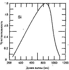
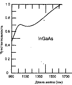
Fig. 6.10. Spectral characteristics of P-i-N-diodes
Response speed
The response rate of the detector is limited by the time of the passage, which is the time overcoming the free charges of the width of the inner layer. This is the function of the reverse displacement voltage and physical width. For quick P-i-N-diodes, it ranges from 1.5 to 10 ns. The capacitance also affects the response of the device, and the transition container forms an insulating inner layer between electrodes formed by P- and N-regions. In high-speed photodiodes, the response time can reach 10 picoseconds with a container of several picofrades with very small surface areas.
Volt-ampere characteristics
Typical voltamper (I - U) curves for a silicon P-i-N-n-n-n-n-n-n-photodium display, in Fig. 6.11. It can be seen that even when there is no optical power, a small reverse current flows, which is called a dark current (Dark Current). It is caused by the temperature formation of free charge carriers, usually doubled every 10 ° C of temperature of temperature after 25 ° C.
Dynamic range
Linear relationship between the voltage and the optical power shown in Fig. 6.11 is usually preserved for about six dozen, giving a dynamic range of about 50 dB.

Fig. 6.11. Voltample characteristics of silicon P-i-N-photoDiode
6.7.3. Construction of P-i-N-photodiodes
The design of P-I-N-photodiodes is similar to those used for LEDs and lasers, but optical requirements are less critical. The active area of \u200b\u200bdetectors is usually much larger than the fiber core, so the transverse alignment does not create problems.
 Magnetometry in the simplest version The ferrozond consists of a ferromagnetic core and two coils on it
 Effective job search course search
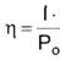 The main characteristics and parameters of the photodiode
 How to edit PDF (five applications to change PDF files) How to delete individual pages from PDF
 Why the fired program window is long unfolded?
 DXF2TXT - export and translation of the text from AutoCAD to display a dwg traffic point in TXT
 What to do if the mouse cursor disappears