Download PCB files in lay format. What program can open the .LAY file? Difference in housings
A simple, yet very effective software package for the design and manual layout of printed circuit boards of small to medium complexity. The program is very popular among Russian radio amateurs.
The main advantage of Sprint-Layout is its intuitive interface, which includes only the most necessary tools for preparing printed circuit boards of 300 x 300 mm. The program allows you to work with two layers (conductors and markings) for each side of the board. Additional features - solder mask layer, metallization, SMD mask. The built-in router only helps you route the wires, and is not automatic. The growing library contains the most common electronic components. Sprint-Layout has the ability to export work results to the popular Excellon and Gerber formats, as well as create an HPGL file for finishing a printed circuit board on a software-controlled milling machine. The package is widely used for.
The program is hardly suitable for professionals, since its capabilities are limited by small boards with low element density. But, thanks to its logical and understandable structure, Sprint-Layout is very easy to learn and is recommended for novice designers who do not want to waste their time learning more complex programs.
The language of the program is German or English. Domestic enthusiasts created a fully functional Russified version of the program, which was named Sprint-Layout 6 on the network (but has nothing to do with the official 6th version, released in 2013). The interface has been redesigned for greater convenience, a large number of electronic components have been added, and compatibility with all original Sprint-Layout versions up to version 5 has been maintained.
You can read about the innovations of the 6th version of Sprint-Layout in the article:

The program works stably in 32- or 64-bit operating systems Windows 98 / ME / NT / 2000 / XP / Vista / Win 7 / Win 8
Distribution of the program: Shareware (paid), price - 40 EUR
Sprint-Layout official website: http://www.abacom-online.de/uk/html/sprint-layout.html
Sprint-Layout file formats: LAY, LAY6, export to Gerber or Excellon
Download Sprint-Layout 6.0 (unofficial Russian version, actually 5.0)
We all love to assemble circuits, but not everyone wants and knows how to lay printed circuit boards. Most often we look for a ready-made seal on the Internet and in most cases we find it. It would seem, go ahead, etch and solder! But not everything is so rosy, because often these found seals look like this:
Not a single signed item. Complete rebus, riddle! And, like, turn on the "mosch" and stuff the elements, because the diagram is at hand. But the program was created to make life easier for us, and not vice versa.
Therefore, I will briefly, from the very beginning, tell you how to approach the layout of the board in Sprint-Layout, so that you do not need to guess later what kind of detail I put in here. Let's get it right right away!
You cannot cover everything in one small article, I will go through some of the main points. So, we create a new project, set the name of the board and the estimated size (it can be easily adjusted later).

Don't forget to choose a suitable work mesh.

For small projects with large elements, a mesh of 1.27 mm is suitable, for more advanced and dense 0.635 mm, and so on. Elements and tracks will be placed with reference to the nodes of this grid. You can make a grid for Soviet parts: 2.5 mm or 1 mm.

Be sure to understand the layer system in the program, understand how everything works, use the photo view.

Make labels on layers for labels, and tracks and polygons on layers for copper, etc.
The archive contains help programs in Russian.
We start adding details to the board. At this stage, the values of "Type" and "Denomination" should not be confused, later I will tell you why.

Enter the values, adjust the font size to taste, click OK.

We see the element with the marking. Now we can distribute and "seal" our markings.
We select the denomination and drag it with the mouse to the desired place. Before that, you need to reduce the size of the grid to an acceptable level.

That's better.

Now move the element designation closer. If necessary, you can rotate it by selecting it before.

Further, so as not to suffer so much with each element, we simply copy it and change the data in the element's properties.

Our board is already quite ready to manufacture, but why do we need to overload the solution with excess copper?
There is no need! We will minimize the area of copper to be vented. To do this, select all the elements on the board and press the "Metallization" button at the bottom of the program window and change the value to an acceptable one, for example 0.5 mm.

Everything is fine, but some legs can and sometimes even need to be placed on a metallized area. There is nothing difficult.

Select the required legs and change the metallization offset value to 0. That's it, now the leg is on the earth bus.

And if you need a thermal barrier to facilitate soldering on large polygons? Select the path drawing and draw the thermal barrier.

This is the simplest and most obvious way. But you can also use the built-in capabilities of the program to create thermal barriers. Highlight the pad you want and study the menu on the right.

Check the "Thermal barrier" checkbox and adjust the direction and width of the "bridges" of the barrier. It is very convenient that many sites can be configured at once. The thermal barrier function works only on the switched on automatic landfill. Not supported by all versions of Sprint-Layout. Use fresh.
Everything is drawn, we can admire the result by pressing the "photoview" button.

A nuance - you can edit the size of the labels of the elements separately, for this, select the "victim" and press the properties button on the right. The settings are pretty extensive. However, it is best to set all decals in the same style.

It was the turn of the "cosmetics". So that all the drawings of the elements on the board have a uniform appearance and line thickness, do the following:
1.select the layer with the marking of the elements;
2. turn off the track layer;
3. select everything (ctrl + A);
4. adjust the thickness of the lines of all elements at the same time;
5. Activate the tracks layer again.


The beauty! By the way, do not forget to adjust the colors of the layers in the program to all taste, to whom my palette seemed gloomy.
Now let us recall the beginning of the article and find out why you should not enter the nominal value of an element in the field for its type. It's simple, it turns out that when we add elements, we have already formed a list of elements!
Of course, the more correct practice is the primacy of the circuit in the project, then the creation of the list of elements is the business of the program for drawing the circuits. In the set of programs from ABACOM it is sPLAN.
Editorial note

It remains only to buy according to the list and get a beautiful home-made board as a result. And people are not ashamed to show such a drawing on the forum, and there will be no unnecessary questions about the board.
Files
And here is the Russian help for Sprint-Layout and an excellent free book by our comrade Mikhail Tsarev (Tsoy73):▼ 🕗 27/12/16 ⚖️ 2.14 Mb ⇣ 168
Updated: 27.04.2016
An excellent amplifier for the home can be assembled on the TDA7294 chip. If you are not strong in electronics, then such an amplifier is ideal, it does not require fine tuning and debugging like a transistor amplifier and is easy to build, unlike a tube amplifier.
The TDA7294 microcircuit has been produced for over 20 years and still has not lost its relevance, and is still in demand among radio amateurs. For a novice radio amateur, this article will be a good help to get acquainted with integrated audio frequency amplifiers.
In this article I will try to describe in detail the amplifier device on the TDA7294. I will focus on a stereo amplifier assembled according to the usual scheme (1 microcircuit per channel) and briefly tell you about the bridge circuit (2 microcircuits per channel).
Chip TDA7294 and its features
TDA7294 - the brainchild of SGS-THOMSON Microelectronics, this microcircuit is an AB class low frequency amplifier, and is built on field-effect transistors.
Of the advantages of the TDA7294, the following can be noted:
- output power, with distortion of 0.3-0.8%:
- 70 W for 4 ohm load, conventional;
- 120W for 8 ohm load, bridged;
- Mute function and Stand-By function;
- low noise level, low distortion, frequency range 20-20000 Hz, wide operating voltage range - ± 10-40 V.
Specifications
| Technical characteristics of the TDA7294 microcircuit | |||||
|---|---|---|---|---|---|
| Parameter | Conditions | Minimum | Typical | Maximum | Units |
| Supply voltage | ± 10 | ± 40 | IN | ||
| Frequency Response Range | Signal 3 db Output power 1W |
20-20000 | Hz | ||
| Long Term Power Output (RMS) | harmonic coefficient 0.5%: Uп = ± 35 V, Rн = 8 Ohm Uп = ± 31 V, Rн = 6 Ohm Uп = ± 27 V, Rн = 4 Ohm |
60 60 60 |
70 70 70 |
W | |
| Peak music output power (RMS), duration 1 sec. | harmonic coefficient 10%: Uп = ± 38 V, Rн = 8 Ohm Uп = ± 33 V, Rн = 6 Ohm Uп = ± 29 V, Rн = 4 Ohm |
100 100 100 |
W | ||
| Total harmonic distortion | Po = 5W; 1kHz Po = 0.1-50W; 20-20000Hz |
0,005 | 0,1 | % | |
| Uп = ± 27 V, Rн = 4 Ohms: Po = 5W; 1kHz Po = 0.1-50W; 20-20000Hz |
0,01 | 0,1 | % | ||
| Protection response temperature | 145 | ° C | |||
| Quiescent current | 20 | 30 | 60 | mA | |
| Input impedance | 100 | kOhm | |||
| Voltage gain | 24 | 30 | 40 | dB | |
| Peak output current | 10 | BUT | |||
| Working temperature range | 0 | 70 | ° C | ||
| Thermal resistance of the case | 1,5 | ° C / W | |||
Pin assignment
| Pin assignment of the TDA7294 microcircuit | |||
|---|---|---|---|
| Chip pin | Designation | Appointment | Connection |
| 1 | Stby-GND | "Signal ground" | "General" |
| 2 | In- | Inverting input | Feedback |
| 3 | In + | Non-inverting input | Audio signal input via coupling capacitor |
| 4 | In + Mute | "Signal ground" | "General" |
| 5 | N.C. | Not used | – |
| 6 | Bootstrap | "Voltodopavka" | Capacitor |
| 7 | + Vs | Input stage power supply (+) | |
| 8 | -Vs | Input stage power supply (-) | |
| 9 | Stby | Standby mode | Control block |
| 10 | Mute | Mute mode | |
| 11 | N.C. | Not used | – |
| 12 | N.C. | Not used | – |
| 13 | + PwVs | Output stage power supply (+) | Positive terminal (+) of the power supply |
| 14 | Out | Exit | Audio signal output |
| 15 | -PwVs | Output stage supply (-) | Minus terminal (-) of the power supply |
Note. The microcircuit case is connected to the minus power supply (pins 8 and 15). Do not forget about isolating the heatsink from the amplifier case or isolating the microcircuit from the heatsink by installing it through a thermal pad.
I also want to note that in my scheme (as in the datasheet) there is no separation of input and output "lands". Therefore, in the description and on the diagram of the definition of "common", "ground", "body", GND should be taken as concepts of the same sense.
Difference in housings
The TDA7294 microcircuit is available in two types - V (vertical) and HS (horizontal). TDA7294V, having a classic vertical design of the case, was the first to leave the assembly line and is still the most common and affordable.

Complex of protection
The TDA7294 chip has a number of protections:
- protection against power surges;
- protection of the output stage against short circuit or overload;
- thermal protection. When the microcircuit is heated to 145 ° C, the Mute mode is activated, and at 150 ° C, the Stand-By mode is activated;
- protection of the microcircuit terminals from electrostatic discharges.
Power amplifier on TDA7294
A minimum of parts in the harness, a simple printed circuit board, patience and known good parts will allow you to easily assemble an inexpensive UMZCH on the TDA7294 with clear sound and good power for home use.
You can connect this amplifier directly to the line-out jack of your computer's sound card. the nominal input voltage of the amplifier is 700 mV. And the level of the nominal voltage of the line output of the sound card is regulated in the range of 0.7-2 V.
Block diagram of the amplifier

The diagram shows a variant of a stereo amplifier. The structure of the bridge amplifier is similar - there are also two boards with TDA7294.
- A0... Power Supply
- A1... Control unit for Mute and Stand-By modes
- A2... UMZCH (left channel)
- A3... UMZCH (right channel)
Pay attention to the connection of the blocks. Improper wiring inside the amplifier can cause additional noise. To minimize noise as much as possible, follow a few rules:
- Power to each amplifier board must be supplied with a separate harness.
- The power wires must be twisted into a pigtail (harness). This will compensate for the magnetic fields created by the current flowing through the conductors. We take three wires ("+", "-", "Common") and weave a pigtail from them with a slight tension.
- Avoid earth loops. This is a situation when the common conductor, connecting the blocks, forms a closed loop (loop). The connection of the common wire should go in series from the input connectors to the volume control, from it to the UMZCH board and further to the output connectors. It is advisable to use connectors isolated from the case. And for input circuits also shielded wires with insulation.
List of parts for PSU TDA7294:

When purchasing a transformer, note that the effective voltage value is written on it - U D, and by measuring with a voltmeter you will also see the effective value. At the output after the rectifier bridge, the capacitors are charged to the amplitude voltage - U A. The amplitude and effective voltages are related by the following relationship:
U A = 1.41 × U D
According to the characteristics of the TDA7294 for a load with a resistance of 4 ohms, the optimal supply voltage is ± 27 volts (U A). The output power at this voltage will be 70 W. This is the optimal power for the TDA7294 - the distortion level will be 0.3–0.8%. It makes no sense to increase the power supply to increase the power. the level of distortion is growing like an avalanche (see graph).

We calculate the required voltage of each secondary winding of the transformer:
U D = 27 ÷ 1.41 ≈ 19 V
I have a transformer with two secondary windings, with a voltage on each winding of 20 volts. Therefore, in the diagram, I designated the power terminals as ± 28 V.
To obtain 70 W per channel, taking into account the efficiency of the microcircuit of 66%, we consider the power of the transformer:
P = 70 ÷ 0.66 ≈ 106 VA
Accordingly, for two TDA7294s, this is 212 VA. The nearest standard transformer, with a margin, will be 250 VA.
Here it is appropriate to state that the power of the transformer is calculated for a pure sine wave signal; corrections are possible for a real musical sound. So, Igor Rogov claims that for a 50 W amplifier, a 60 VA transformer will be enough.
The high-voltage part of the power supply unit (up to the transformer) is assembled on a 35 × 20 mm printed circuit board;

The low-voltage part (A0 according to the structural diagram) is assembled on a 115 × 45 mm printed circuit board:

All amplifier boards are available in one.
This power supply unit for TDA7294 is designed for two microcircuits. For more microcircuits, it will be necessary to replace the diode bridge and increase the capacitance of the capacitors, which will entail a change in the dimensions of the board.
Control unit for Mute and Stand-By modes
The TDA7294 microcircuit has Stand-By and Mute modes. These functions are controlled through pins 9 and 10, respectively. The modes will be turned on as long as there is no voltage at these pins or it is less than +1.5 V. To "wake up" the microcircuit, it is enough to apply a voltage greater than +3.5 V to pins 9 and 10.
For the simultaneous control of all UMZCH boards (especially important for bridge circuits) and saving radio components, there is a reason to assemble a separate control unit (A1 according to the structural diagram):

Parts list for control box:
- Diode (VD1)... 1N4001 or similar.
- Capacitors (C1, C2)... Polar electrolytic, domestic K50-35 or imported, 47 μF 25 V.
- Resistors (R1 – R4)... Normal low-power.
The printed circuit board of the block has dimensions of 35 × 32 mm:

The task of the control unit is to provide silent switching on and off of the amplifier due to the Stand-By and Mute modes.
The principle of operation is as follows. When you turn on the amplifier, together with the capacitors of the power supply, the capacitor C2 of the control unit is also charged. As soon as it is charged, the Stand-By mode will turn off. The capacitor C1 takes a little longer to charge, so the Mute mode will turn off in the second turn.
When the amplifier is disconnected from the mains, the capacitor C1 is discharged first through the VD1 diode and turns on the Mute mode. Then the capacitor C2 discharges and sets the Stand-By mode. The microcircuit becomes silent when the capacitors of the power supply have a charge of about 12 volts, so no clicks and other sounds are heard.
Amplifier on TDA7294 in the usual way
The circuit for switching on the microcircuit is non-inverting, the concept corresponds to the original from the datasheet, only the ratings of the components have been changed to improve the sound characteristics.
Parts List:
- Capacitors:
- C1... Film, 0.33-1 μF.
- C2, C3... Electrolytic, 100-470 μF 50 V.
- C4, C5... Film, 0.68 μF 63 V.
- C6, C7... Electrolytic, 1000 μF 50 V.
- Resistors:
- R1... Variable double with linear characteristic.
- R2 – R4... Normal low-power.
Resistor R1 is double because amplifier stereo. Resistance no more than 50 kOhm with linear, not logarithmic characteristic for smooth volume control.
The R2C1 circuit is a high-pass filter (HPF), suppresses frequencies below 7 Hz, without passing them to the amplifier input. Resistors R2 and R4 must be equal to ensure stable operation of the amplifier.
Resistors R3 and R4 organize a negative feedback circuit (OOS) and set the gain:
Ku = R4 ÷ R3 = 22 ÷ 0.68 ≈ 32 dB
According to the datasheet, the gain should be within 24-40 dB. If less, then the microcircuit will self-excite, if more, distortion will grow.
Capacitor C2 participates in the OOS circuit, it is better to take with a larger capacity in order to reduce its effect on low frequencies. Capacitor C3 provides an increase in the supply voltage of the output stages of the microcircuit - "voltage boost". Capacitors C4, C5 eliminate wire induced noise, and C6, C7 complement the filter capacity of the power supply. All amplifier capacitors, except C1, must have a voltage margin, so we take at 50 V.
The printed circuit board of the amplifier is one-sided, rather compact - 55 × 70 mm. When developing it, the goal was to dilute the "earth" with a star, to ensure versatility and at the same time keep the minimum dimensions. I think this is one of the smallest boards for the TDA7294. This board is designed for the installation of one microcircuit. For the stereo version, respectively, two boards are required. They can be installed side by side or one above the other like mine. I'll tell you more about versatility a little later.

The radiator, as you can see, is indicated on one board, and the second, similar, is attached to it from above. Photos will be a little further.
Amplifier on the TDA7294 bridge circuit
The bridge circuit is a pairing of two conventional amplifiers with some amendments. Such a circuit solution is designed to connect acoustics with an impedance of not 4, but 8 ohms! The acoustics are connected between the outputs of the amplifiers.
There are only two differences from the usual scheme:
- the input capacitor C1 of the second amplifier is connected to ground;
- added feedback resistor (R5).
The printed circuit board is also a combination of amplifiers in the usual way. The board size is 110 × 70 mm.

Universal board for TDA7294
As you may have noticed, the aforementioned boards are essentially the same. The next PCB option fully confirms the versatility. This board can be used to assemble a 2 × 70 W stereo amplifier (conventional circuit) or a 1 × 120 W mono amplifier (bridged). Board size - 110 × 70 mm.


Note. To use this board in a bridged version, you must install the resistor R5, and set the jumper S1 in the horizontal position. In the figure, these elements are shown with a dotted line.
For a conventional circuit, the resistor R5 is not needed, and the jumper must be installed vertically.
Assembly and commissioning
Assembling the amplifier is straightforward. As such, the amplifier does not require adjustment and will work immediately, provided that everything is assembled correctly and the microcircuit is not defective.
Before using for the first time:
- Make sure the radio components are installed correctly.
- Check that the power wires are connected correctly, do not forget that on my amplifier board, the "ground" is not in the center between the plus and minus, but on the edge.
- Make sure that the microcircuits are isolated from the heatsink, if not, check that the heatsink does not contact ground.
- Apply power to each amplifier in turn, so there is a chance not to burn all the TDA7294s at once.
First turn on:
- We do not connect the load (acoustics).
- We short-circuit the inputs of the amplifiers to ground (short-circuit X1 with X2 on the amplifier board).
- We serve food. If everything is fine with the fuses in the power supply unit and nothing smokes, then the launch was successful.
- Using a multimeter, we check the absence of direct and alternating voltage at the output of the amplifier. A slight constant voltage is allowed, no more than ± 0.05 volts.
- We turn off the power and check the case of the microcircuit for heating. Be careful, the capacitors in the power supply take a long time to discharge.
- We give a sound signal through a variable resistor (R1 according to the scheme). We turn on the amplifier. The sound should appear with a short delay, and immediately disappear when turned off, this characterizes the operation of the control unit (A1).
Conclusion
I hope this article will help you build a quality amplifier based on the TDA7294. Finally, I present a few photos during the assembly process, do not pay attention to the quality of the board, the old PCB was etched unevenly. As a result of the assembly, some edits were made, so the boards in the .lay file are slightly different from the boards in the photographs.


The amplifier was made for a good friend, he invented and implemented such an original case. Photos of the TDA7294 stereo amplifier assembly:


On a note: All printed circuit boards are collected in one file. To switch between "seals", click on the tabs as shown in the figure.

list of files
Multimedia amplifier based on TDA1554 2.1
This amplifier is designed to create a 2.1 system, i.e. 2 broadband amplifiers + 1 more powerful, designed to reproduce only low frequency signals.
The schematic diagram of the amplifier is shown in Figure 1, the drawing of the printed circuit board is shown in Figure 2 (not to scale). You can take a drawing in lay format.
Picture 1.

Figure 2. DOWNLOAD THE BOARD IN LAY
PCB FOR HIGH QUALITY POWER AMPLIFIER
This multimedia amplifier is designed to create a mid-range audio system designed for stationary use.
The amplifier is based on the popular TDA2030 microcircuits and the not very popular TDA2052. Well, since we are talking about these microcircuits, it is better to dwell in more detail on each of them.
According to the reference book, the TDA2030 belongs to the category of Hi-Fi amplifiers, but this is said to be too loud - its sound is somewhat non-Hi-Fi. Its more powerful brother, the TDA2050, sounds much nicer. In terms of pinout, it completely coincides with the TDA2030, so you can replace it without changing almost anything on the PCB.
The schematic diagram of the amplifier on the TDA2030 microcircuit is shown in Figure 1, in Figure 2 - TDA2050 - drawing and imported from the datasheet. The only thing that has been changed in the circuit is that there are no diodes from the m / s output to plus or minus power supply. These diodes are used to reduce the self-induction of the dynamic head, and few people will decide to use this circuit with heads with a "heavy" diffuser, then the diodes were simply excluded from the circuit. A large batch of boards produced without these diodes showed that the amplifier works as stably as with them, i.e. the operation of the scheme was not influenced.

Picture 1.

Figure 2.
Of course, the ratings in the OOS circuit are different, but their ratio is almost the same, which means coffee. they have the same gain. In addition, the TDA2050 OOS option is more preferable, since more current flows through smaller resistors, therefore, it is less critical to pickups and external interference. And yet - we allowed ourselves to bypass R5 with a series-connected 100 kΩ resistor and a 100 pF capacitor. This increases the stability of the amplifier and provides a roll-off of the coffee. amplification at frequencies above 20 kHz.
The power supply of the amplifier is chosen unipolar since there is almost no deterioration in sound quality, but this fact opens additional horizons:
- there is some savings in electrolytic capacitors for power supply;
- when creating a multimedia amplifier using a bipolar power supply, the positive "branch" of the power supply is used to power the midrange-RF link as an amplifier with a unipolar power supply, and the positive and negative "branches" are used as the power supply of the amplifier for the subwoofer. Thus, the amplifier circuitry is rather not badly simplified.
If there is no desire to bother with a bipolar, then you can use a bridge connection of microcircuits, just give a correction for the fact that in a bridge connection much more power is required from m / s. For example, when using the MF-HF link with the TDA2030, the bridge amplifier should be used with the TDA2050, but if the MF-HF amplifiers are based on the TDA2050 chip, then the bridge amplifier must already be taken on the basis of the TDA2052.
Figure 3 shows a sketch of a printed circuit board for one TDA2030.

Figure 3. DOWNLOAD IN LAY

Well, a few words about the amplifier on the TDA2052 microcircuit. This is an integrated power amplifier that allows you to develop at a load of 4 ohms up to 40 watts. The schematic diagram of the amplifier is shown in Figure 4.

Figure 4.
This is an amplifier with two inputs, but to simplify the design, the second input is simply not used. A sketch of the printed circuit board is shown in Figure 5. Figure 6 is a sketch of the TDA2052 bridge connection, but Figure 7 is a sketch of the printed circuit board of the TDA2030 (TDA2050) multimedia amplifier itself and the TDA2052 bridge amplifier.
The drawing of the printed circuit board of the power amplifier is one for all - DOWNLOAD.

Figure 5.

Figure 6.

Figure 7.
Integrated four-channel power amplifiers.
How to quickly assemble an amplifier for 4 channels, and at the same time they are not afraid to repair automotive equipment will be told here ...
We are talking about a number of microcircuits that have one switching circuit, but different characteristics. Of course, they also have one signet. Well, let's start in order:
In automotive technology, the TDA7381, TDA7382, TDA7383, TDA7384, TDA7385, TDA7386 microcircuits are often used, somewhat less often TDA7560. All these monsters practically have one switching circuit, shown in Figure 1, but their characteristics differ somewhat, which is actually reflected in Table 1.

Picture 1.
TABLE 1.
| PARAMETER |
PARAMETER FOR MICROCIRCUIT |
||||||
| Type of shell |
FLEXIWATT25 |
||||||
| Gain cof, dB | |||||||
| Supply voltage, V | |||||||
| Output power at THD 10% |
25 45 |
||||||
| Output power at THD 1% |
19 34 |
||||||
| Maximum output power (a rectangular signal with an amplitude of 100 mV is fed to the input), this is what is written on the "muzzles" of the radio tape recorders. |
50 80 |
||||||
| THD,%, at P = 4W | |||||||
| Input impedance, kOhm | |||||||
| Diagnostics, pin 25 is enabled. | |||||||
| Voltage at the control inputs MUTE and St-By for switching on to the operating mode, not less, V | |||||||
| Blue indicates the parameters for a load of 2 Ohms, please note that only TDA7560 can work with 2 Ohms (!) | |||||||
| One nuance is indicated in pink - these microcircuits have a diagnostic output, which is fed to the central processor and if it is used in the radio tape recorder, then the microcircuit can only be replaced with a diagnostic output, otherwise the CPU simply will not give permission for the volume and tone control, and some may generally will not turn on ... Well, for the manufacture of a separate amplifier, this does not matter. | |||||||

Well, what kind of mikruhi they sort of figured out, now the printed circuit boards for this four-channel:

Figure 2.
Figure 2 shows a sketch of a printed circuit board, a drawing in lay format, in jpg, in jpg, the drawing is already expanded, i.e. prepared for laser iron. J1 jumper is spaced in height, I just didn't want to drag ultra-thin tracks between the pins, and it's not serious to make a double-sided board for such a primitive either ... You can read a little more about TDA7384 and TDA7560.
The microcircuits are heated quite well, and at least the operating temperature is more than 100 degrees. Intact. it is better not to skimp on a radiator.
And finally, a couple of words about the miracle that I was able to see, namely the very original use of the amplifier on the TDA7560 in the car. 4 loudspeakers 25GDN are installed in an absolutely flat case, the height of which is about 170 mm. Length and width are tailored to the size of the classic trunk. The bass reflex is installed. The speakers are connected in parallel in pairs, i.e. load 2 Ohms and connected to the two outputs of the TDA7560. The remaining pair of outputs are connected to paired JBLs with a diameter of 160mm, i.e. another stereo set of 2 ohms, installed in the rear shelf. Front acoustics from JVC head.
I really liked the train of thought of this needleman - there is no pipe of unmeasured dimensions lying around the trunk, there is about 200 real watts and this is without any converters ... True, the radiator of the mirkruha with some kind of stationary amplifier looks like Lortovsky, only it seems like it is higher ...
PCB FOR MULTIMEDIA AMPLIFIER ON TDA1554 & TDA1562
This multimedia amplifier is designed to create a mediocre audio system and can be used both in the car and in the hospital.
The main disadvantage of the system is the somewhat underestimated value of the boost capacitors, although the schematic diagrams of both amplifiers are taken from the datasheet - Figures 1 and 2.

Picture 1.

Figure 2.
In reality, the low frequency sound becomes much better when using C1 and C2 at 10000mkF, but they did not bring the board to the "mind" ...
By the way, nothing bothers you, having slightly corrected the board, make a separate amplifier on the TDA1554 or TDA1562.
Figure 3 shows a drawing of the board (not to scale), the same in lay format.

Figure 3.
You can see the details of how much power a power supply is needed for a power amplifier in the video below. The STONECOLD amplifier is taken as an example, but this measurement gives an understanding that the power of the mains transformer can be less than the power of the amplifier by about 30%.
Site administration address:
DIDN'T FIND WHAT YOU ARE LOOKING FOR? DROWNED:
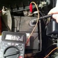 Simple tips on how to test a transformer with a multimeter for operability
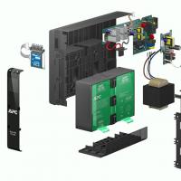 Repair of uninterruptible power supplies Commercial proposal for the repair of an uninterruptible power supply
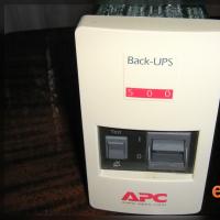 Do-it-yourself UPS repair: wizard's advice Repair of apc uninterruptible power supplies
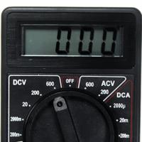 Repair of a multimeter m 830b does not show an ohmmeter
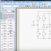 Programs for drawing electrical circuits
 Drawing boards in Sprint-Layout correctly from the first steps
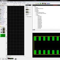 What program can open the file