GeForce 9800 What Series. We define a NVIDIA video card product. Pros and Cons Video Card
| NVIDIA GeForce 9000 Series | |
|---|---|
| Code name | G92, G92B, G94, G94B, G96, G98 |
| GPU entry level | GeForce 9300GS, GeForce 9400GT, GeForce 9500GT |
| GPU medium range | GeForce 9600. |
| Top GPU. | GeForce 9800. |
| Version of Direct3D and shaders | Direct3D 10. Shader Model 4.0. |
| OpenGL version | OpenGL 3.3. |
| OpenCL version | OpenCl 1.1. |
| Predecessor | GeForce 8. |
| Successor | GeForce 100. |

NVIDIA GeForce 9800 GX2

Gigabyte GeForce 9500 GT
Technical Specifications GeForce 9 Series
| Model | 9800 | 9600 | 9500 | 9400 | 9300 | |||||||
|---|---|---|---|---|---|---|---|---|---|---|---|---|
| GX2. | GTX +. | GTX. | GT. | GT Green. | GT. | GT Green. | GSO 512. | GSO. | GT. | GT. | GS. | |
| release date | 18.03.08 | 18.07.08 | 01.04.08 | 18.07.08 | - | 21.02.08 | - | - | 29.04.08 | 18.07.08 | 26.08.08 | - |
| Graphic processor | 2 x G92. | G92B. | G92. | G92B. | G94. | G94B. | G94. | G92. | G96. | G98. | ||
| Number of transistors, million | 2 x 754. | 754 | 505 | 754 | 314 | - | ||||||
| TEHPROTSESS, NM | 65 | 55 | 65 | 65 / 55 | 55 | 65 / 55 | 55 | 65 | 55 | 65 | ||
| Core frequency, MHz | 600 | 738 | 675 | 600 | 550 | 650 | 600 | 650 | 550 | 567 | ||
| Frequency of the Shader Block, MHz | 1500 | 1836 | 1688 | 1512 | 1375 | 1625 | 1500 | 1625 | 1375 | 1400 | ||
| Number of streaming processors | 2 x 128. | 128 | 112 | 64 | 48 | 96 | 32 | 16 | 8 | |||
| Number of textural blocks | 2 x 64. | 64 | 56 | 32 | 24 | 48 | 16 | 8 | ||||
| Number of rasterization blocks | 2 x 16. | 16 | 12 | 8 | 4 | |||||||
| Performance, Gflops. | 2 x 576. | 705 | 648 | 504 | 462 | 312 | 288 | 234 | 396 | 134,4 | 67,2 | 33,6 |
| Filling the scene, billion pixes / | 2 x 9.6 | 11,8 | 10,8 | 9,6 | 8,8 | 10,4 | 9,6 | 7,8 | 6,6 | 4,4 | 2,2 | |
| Filling the scene, billion tex / | 2 x 38.4 | 47,2 | 43,2 | 33,6 | 30,8 | 20,8 | 19,2 | 15,6 | 26,4 | 8,8 | 4,4 | 4,5 |
| Standard video memory | GDDR3 | DDR2. | ||||||||||
| Blossomy Tires video memory, bit | 2 x 256. | 256 | 192 | 128 | 64 | |||||||
| Frequency of video memory, MHz | 1000 | 1100 | 900 | 800 | 500 | |||||||
| Memory bandwidth, GB / | 2 x 64.0. | 70,4 | 57,6 | 38,4 | 16,0 | 8,0 | ||||||
| Volume of video memory, MB | 2 x 512. | 512 / 1024 | 512 | 384 | 512 | 256 | ||||||
| Power consumption, W. | 265 | 140 | 165 | 105 | 75 | 95 | 60 | 90 | 100 | 50 | 30 | |
| Interface | PCI Express 2.0 x16 | |||||||||||
| Support versions API | Direct3D 10, OpenGL 3.3, OpenCL 1.1 | |||||||||||
| Support version of Shader Model | Shader Model 4.0. | |||||||||||
GEFORCE 9800 Series
NVIDIA GeForce 9800GX2.
- Tire PCI Express 2.0;
- Two graphics cores G92-450 (65-nm) operating at a frequency of 600 MHz;
- 256 (2 × 128) streaming processors operating at a frequency of 1500 MHz;
- 1024 MB (2 × 512 MB) GDDR3 video memory with a 256-bit interface and a frequency of 1000 MHz;
- Power consumption is 265 W;
- Compatibility with DirectX 10 .0 Shader Model 4.0 OpenGL 3.3;
- Support Quad SLI.
In fact, a double card based on a pair of 8800gts 512 MB. This video card is a continuation of the GX2 two-phase accelerators concepts, which were found in the NVIDIA GeForce 7900 series.
NVIDIA GeForce 9800GTX +
- Tire PCI Express 2.0;
- Graphic core G92B-400 (55-nm) operating at a frequency of 738 MHz;
- 128 streaming processors operating at a frequency of 1836 MHz;
- 1024 MB or 512 MB GDDR3
- Power consumption is 140 W;
- Support 3-way SLI.
It is a version of GeForce 9800GTX on a 55-nm technical process with increased frequencies and less power consumption. In terms of performance, a little exceeds AMD / ATI Radeon 4850. Later was renamed GeForce GTS 250.
NVIDIA GeForce 9800GTX
- Tire PCI Express 2.0;
- Graphic core G92-400 (65-nm) operating at a frequency of 675 MHz;
- 128 streaming processors operating at a frequency of 1688 MHz;
- 1024 MB or 512 MB GDDR3 video memory with a 256-bit interface and a frequency of 1100 MHz;
- Power consumption is 168 W;
- Compatibility with DirectX 10.0 Shader Model 4.0 OpenGL 3.3;
- Support 3-way SLI.
Analogue NVIDIA GeForce 8800GTS 512 MB with elevated frequencies. Very quickly lost its place in the 9800GTX + market, urgently released in response to the AMD / ATI Radeon 4850/4870 exit, which have a higher productivity.
NVIDIA GeForce 9800GT.
- Tire PCI Express 2.0;
- The G92-400 graphics core (65-nm / 55-nm) operating at a frequency of 600 MHz;
- 112 streaming processors;
- 1024 MB or 512 MB GDDR3
- Power consumption is 105 W;
- Compatibility with DirectX 10.0 Shader Model 4.0 OpenGL 3.3;
- Support 2-way SLI.
Analogue NVIDIA GeForce 8800GT 512 MB.
NVIDIA GeForce 9800GT Green
- Tire PCI Express 2.0;
- Graphics core G92-400 (55-nm) operating at a frequency of 550 MHz;
- 112 streaming processors;
- 1024 MB or 512 MB GDDR3 video memory with a 256-bit interface;
- Power consumption is 75 W;
- Compatibility with DirectX 10.0 Shader Model 4.0 OpenGL 3.3;
- Support 2-way SLI.
The NVIDIA GeForce 9800 GT video adapter with a capacity of 512 MB appeared on the market in 2008, replacing the previous model. Later, versions with 1 GB GDDR5 were released and improved features in games. All options of maps were in the budget price category and were intended to build inexpensive game computers.
The parameters of the graphics adapter fully comply with the requirements of the 2008-2009 game applications. The main characteristics of NVIDIA GeForce 9800 GT are as follows:
- G92-270 graphics processor;
- GPU frequency - from 550 to 600 MHz;
- Memory frequency - 1400-1800 MHz;
- Bigness - 256 bits;
- Maximum data transfer rate - 57.6 GB / s;
- Supported image resolution - up to 2560x1600.
The video card supports NVIDIA SLI technology to improve performance, HybridPower to automatically switch to embedded graphics and physx, which ensures maximum realistic gaming process. It also works with DirectX 10 and OpenGL 2.0 packages, providing high-quality 3D graphics. Support for more modern sets of the functions API is not provided.
GEFORCE 9800 GT Overview
Energy consumption 9800 GT is quite high - at 105 W, so it requires a powerful power supply unit. The manufacturer recommends using at least 450 W. To launch modern games it is worth choosing more productive BP - by 500 or 600 W.
In order to maintain the normal temperature of the GEFORCE 9800 GT video card, all modifications are completed with active cooling systems - as a rule, with one cooler.
In normal mode, the card is heated no more than 77 degrees. The maximum value is 105 degrees.
To connect peripheral devices on the video adapter, there are such connectors:
- 2 DVI, which can be connected through adapters and conventional VGA and HDMI cables;
- TV-out to output analog signal;
- Mio, with which you can combine two cards.
The maximum value of the effective frequency of the video card is 2000 MHz, which allows you to overclock it by 11-30%, depending on the model. It is worth considering that a noticeable increase in indicators can lead to severe overheating.
How to overclock the NVIDIA GeForce 9800 GT video card

Performing an NVIDIA GeForce 9800 GT acceleration, you can increase the value of its frequency. The result becomes an increase in the performance of the card and FPS during the gameplay. Although run games, the minimum requirements of which it does not match, it will not work anyway.
Ensure the NVIDIA GeForce 9800 GT video card acceleration will help special utilities of the MSI AfterBurner or NVIDIA Inspector.
The maximum frequency of the overclocked video adapter should not exceed 2000 MHz. The overclocked card works faster, but consumes up to 120-125 W.
After overclocking mining on the 9800 GT is possible, but not recommended. Even with the advent of the new Bitcoin Gold cryptocurrency, which can be obtained using graphic processors, performance will still be too low even in order to recoup electricity, especially with such a high TDP.
What games will pull NVIDIA GeForce 9800 GT

The test in the GEFORCE 9800 GT tests spent at one time showed the possibility of using a video card for budgetary Gamers. Minimum requirements for a computer corresponding to the map: Motherboard with PCI-Express 16x, 512-1024 MB of RAM and 500 W power supply. Also recommended installation package DX10.
The check results are as follows:
- In the CRYSYS (2009) game when installing a resolution of 1280 × 1024 pix. The 512-megabyte model provides from 22 to 30 FPS - approximately at the HD 4770 video card level.
- When you start the game STALKER (resolution of 1680x1050 pix.) The change frequency of the pictures reaches 13-25 frames per second, if you use the adapter with 512 MB GDDR5, and up to 30, if you install a gigabyte version on the computer.
- Skyrim with 512 MB card will not start at all, and gigabyte modification on the minimum settings will show up to 65 FPS.
Games released after 2011-2012, run with the help of GeForce 9800 GT 512 MB is not recommended. Most of them will show no more than 20 fps, the rest will not work. The version with 1 GB of memory is suitable, but also hardly ensure the valid quality of the gameplay.
Comparison of manufacturers
At the very beginning of sales, the NVIDIA GeForce 9800 GT price was about 2700-3000 rubles per version with 512 MB and about 3.5 thousand rubles. For gigabyte modifications. Products of more well-known manufacturers like MSI, Palit and ASUS received a memory frequency of 1800 MHz and a higher cost. Now it can be bought in the secondary market for only 600-700 rubles.
| Mark. | Memory, MB | Processor frequency, MHz | Memory frequency, MHz | Cost, rub. |
|---|---|---|---|---|
| Gigabyte | 1024 | 600 | 1800 | 3600 |
| Gigabyte | 512 | 600 | 1500 | 2900 |
| Gigabyte | 512 | 550 | 1800 | 2800 |
| ECS. | 512 | 550 | 1800 | 2600 |
| MSI | 512 | 550 | 1800 | 2900 |
| ASUS | 512 | 600 | 1800 | 3000 |
| Inno3d. | 1024 | 600 | 1800 | 3500 |
| Club 3D | 1024 | 550 | 1400 | 3300 |
| Gainward | 1024 | 550 | 1800 | 3500 |
| Zotac | 1024 | 550 | 1600 | 3400 |
| Palit. | 512 | 600 | 1800 | 2700 |
| Palit. | 1024 | 550 | 1800 | 3400 |
More favorable variants of ZOTAC brands, Club 3D and Gigabyte managed to buyers cheaper, but also worked slower. The frequency of such graphics adapters was within 1400-1600 MHz. Now their price is about the same as for models once worthwhile - no more than 1000 rubles.
How to reinstall the video driver for GeForce 9800 GT
For normal operation of the video adapter, you need to have properly running managers. There are three ways to download and install new drivers on a computer with a 9800 GT card:
- Download from the official resource of the manufacturer. The only option that guarantees the right job and PC security.
- Download from third-party resources. The method at which you can not only download the driver for NVIDIA GeForce 9800 GT, but also infect the computer with a virus.
- Using special DRIVERPACK SOLUTION, DriverHub or Driver Booster FREE utilities. In this case, the driver may be obsolete.
On the official website of NVIDIA, you can find new versions of control programs for the video cards intended for various operating systems. The list of supported platform card has Windows 7 32 and 64 bits, Windows 10 and Linux. On other resources you can find drivers for rare OS such as Solaris.
TV-in (need capture chip)
2 x DVI Dual Link
HDTV-Out.
TV-in (need capture chip)
2 x DVI Dual Link
HDTV-Out.
HDMI
TV-in (need capture chip)
2 x DVI Dual Link
HDTV-Out.
HDMI
DisplayPort.
FP16.
I8.
DXTC, S3TC.
3dc.
FP16.
I8.
10
Others
CSAA 2X-16X
optimization of geometric shadows
Specifications of reference cards based on the G8X family
| map | chip tire | ALU / TMU blocks | nuclear Frequency (MHz) | memory frequency (MHz) | memory size (MB) | PSP (GB) | texel Rate (Mtex) | phil Rate (MPIX) |
| GeForce 8500 GT. | G86 Peg16x | 16/8 | 450 | 400(800) | 256 DDR2. | 12.8 (128) | 3600 | |
| GeForce 8600 GT. | G84. Peg16x | 32/16 | 540 | 700(1400) | 256 GDDR3 | 22.4 (128) | 8600 | 4300 |
| GeForce 8600 GTS. | G84. Peg16x | 32/16 | 675 | 1000(2000) | 256 GDDR3 | 32.0 (128) | 10800 | 5400 |
| GeForce 8800 GTS 320MB | G80. Peg16x | 96/24 | 500 | 800(1600) | 320 GDDR3. | 64.0 (320) | 12000 | 10000 |
| GeForce 8800 GTS 640MB | G80. Peg16x | 96/24 | 500 | 800(1600) | 640 GDDR3 | 64.0 (320) | 12000 | 10000 |
| GeForce 8800 GTX | G80. Peg16x | 128/32> | 575 | 900(1800) | 768 GDDR3 | 86.4 (384) | 18400 | 13800 |
| GeForce 8800 Ultra. | G80. Peg16x | 128/32 | 612 | 1080(2160) | 768 GDDR3 | 104.0 (384) | 19600 | 14700 |
| GeForce 8800 GT 256MB | G92. Peg16x | 112/56 | 600 | 700(1400) | 256 GDDR3 | 44.8 (256) | 33600 | 9600 |
| GeForce 8800 GT 512MB | G92. Peg16x | 112/56 | 600 | 900(1800) | 512 GDDR3 | 57.6 (256) | 33600 | 9600 |
| GeForce 8800 GTS 512MB | G92. Peg16x | 128/64 | 650 | 1000(2000) | 512 GDDR3 | 64.0 (256) | 41600 | 10400 |
| GeForce 8800 GS. | G92. Peg16x | 96/48 | 550 | 800(1600) | 384 GDDR3. | 38.4 (192) | 26400 | 6600 |
| GeForce 9400 GT. | G96. Peg16x | 16/8 | 550 | 800(1600) | 256/512 GDDR2. | 25.6 (128) | 4400 | 4400 |
| GeForce 9500 GT. | G96. Peg16x | 32/16 | 550 | 800(1600) | 256/512 GDDR2 / GDDR3 | 25.6 (128) | 8800 | 4400 |
| GeForce 9600 GSO. | G92. Peg16x | 96/48 | 550 | 800(1600) | 384 GDDR3. | 38.4 (192) | 26400 | 6600 |
| GeForce 9600 GT. | G94. Peg16x | 64/32 | 650 | 900(1800) | 512 GDDR3 | 57.6 (256) | 20800 | 10400 |
| GeForce 9800 GT. | G92. Peg16x | 112/56 | 600 | 900(1800) | 512 GDDR3 | 57.6 (256) | 33600 | 9600 |
| GeForce 9800 GTX | G92. Peg16x | 128/64 | 675 | 1100(2200) | 512 GDDR3 | 70.4 (256) | 43200 | 10800 |
| GeForce 9800 GTX + | G92. Peg16x | 128/64 | 738 | 1100(2200) | 512/1024 GDDR3 | 70.4 (256) | 47200 | 11800 |
| GeForce 9800 GX2. | 2xG92. Peg16x | 2x (128/64) | 600 | 1000(2000) | 2x512 GDDR3 | 2x64.0. (2x256) | 76800 | 19200 |
| GeForce GTS 250. | G92. Peg16x | 128/64 | 738 | 1100(2200) | 512/1024 GDDR3 | 70.4 (256) | 47200 | 11800 |
| map | chip tire | ALU / TMU blocks | nuclear Frequency (MHz) | memory frequency (MHz) | memory size (MB) | PSP (GB) | texel Rate (Mtex) | phil Rate (MPIX) |
Details: G80, family GeForce 8800
Specifications G80
- Official name of the chip GeForce 8800
- Code name G80.
- Technology 90 nm
- 681 million transistors
- Unified architecture with an array of common processors for streaming vertices and pixels, as well as other possible types of data
- Hardware support for the latest DirectX 10 innovations, including a new shader model - Shader Model 4.0, generating geometry and recording intermediate data from shaders (Stream Output)
- 384 bits of the memory bus, 6 independent 64 bit width controllers, support for GDDR4
- 575 GHz core frequency (GeForce 8800 GTX)
- 128 scalar alu floating point (integer and floating formats, support for FP 32-bit accuracy within the framework of the IEEE 754 standard, Mad + Mul without loss of clocks)
- ALU operate on more than double frequency (1.35 GHz for 8800 GTX)
- 32 texture block, support FP16 and FP32 component in textures
- 64 block of bilinear filtering (i.e., free honest trilinear filtering is possible, as well as twice the speed of anisotropic filtering)
- - Size of the planning unit - 8x4 (32) pixels.
- 6 wide ROP blocks (24 pixels) with support for anti-aliasing modes up to 16 samples on pixel including at FP16 or FP32 Frame buffer format (i.e., HDR + AA). Each block consists of an array of flexiblely configurable ALU and is responsible for generating and comparing Z, MSAA, blending. Peak performance of the entire subsystem to 96 MSAA samples (+ 96 Z) for the tact, in the mode without color (z only) - 192 references for the tact.
- All interfaces are deposited on an external additional NVIO chip (2 RAMDAC, 2 Dual DVI, HDMI, HDTV)
- Very good architecture scalability, you can block one block or remove memory controllers and ROP (only 6), shader blocks (only 8 TMU + ALU blocks)
GEFORCE 8800 GTX Reference Card Specifications
- Core frequency 575 MHz
- The frequency of universal processors 1350 MHz
- Number of textural blocks - 32, Blocks of blending - 24
- Memory capacity 768 megabytes
- Bandwidth of memory 86.4 gigabyte in sec.
- Theoretical Maximum Tormal Speed \u200b\u200bof 13.8 Gigapixel in Sec.
- Theoretical selection speed of 18.4 gigatexel textures per second.
- SLI connector
- Tire PCI-Express 16x
- Recommended Price $ 599
GEFORCE 8800 GTS reference card specification
- Core frequency 500 MHz
- Frequency of universal processors 1200 MHz
- Number of universal processors 96
- Number of textural blocks - 24, Blocks of blending - 20
- GDDR3 memory type, 1.1 ns (regular frequency 2 * 900 MHz)
- Memory capacity 640 megabytes
- Theoretical Maximum Tormal Speed \u200b\u200b10.0 Gigapixel in Sec.
- Theoretical Sampling Sample Textures 12.0 Gigateksle in Sec.
- Two DVI-I connectors (Dual Link, supported in permissions up to 2560x1600)
- SLI connector
- Tire PCI-Express 16x
- TV-Out, HDTV-OUT, HDCP support
- Recommended price $ 449
Architecture
Transition to unified graphic architectures We waited long. Now you can state the fact - with the advent of GeForce 8800 this transition happened, and the critical peak is already passed. Further will follow the gradual descent of such architectures in the middle and budget segments and their further development, up to a merger with multi-core processor architectures in the distance perspective. So, we get acquainted with the first unified architecture from NVIDIA:
Before us is the whole diagram of chip. The chip consists of 8 universal computing blocks (shader processors) and although NVIDIA speaks of 128 processors, stating that each ALU is such, it is somewhat incorrect - the command execution unit is such a processoring unit in which 4 TMU and 16 ALU are grouped. In total, in this way, we have 128 ALU and 32 TMUs, but the granularity of execution is 8 blocks, each of which can be engaged in one moment, for example, to perform a part of a vertex, or pixel, or a geometric shader over a block of 32 pixels (or A block from the corresponding number of vertices and other primitives). All branches, transitions, conditions, etc. It is used entirely to one block and thus the logical of everything, and to be called a shader processor, let and very wide.
Each such processor is equipped with its own first level cache, in which not only textures are now stored, but also other data that may be requested by a shader processor. It is important to understand that the main flow of data, such as pixels or vertices, which are processed, moving in a circle under the control of gray cardinal (block marked on the Thread Processor scheme) - are not cached, but go to the stream, which is the main charm of today's graphic Architectures - the absence of a completely accidental access at the level of processed primitives.
In addition to the control unit and 8 computing shader processors, in stock 6 ROP blocks that execute visibility definitions, write to the frame buffer and MSAA (blue, next to the L2 cache blocks) grouped with memory controllers, check queues and a second-level cache.
Thus, we got a very wide (8 blocks processing portions of 32 pixels each) architecture can smoothly scalle in both directions. Adding or removing memory controllers and shader processors will appropriately scale the bandwidth of the entire system without disturbing the balance and without creating bottlenecks. This is a logical and beautiful solution that implements the main plus of a unified architecture is an automatic balance and high efficiency of the use of available resources.
In addition to shader blocks and ROPs, a set of managers and administrative blocks:
- Blocks that run on execution data of certain formats (VERTEX, Geometry and Pixel Thread Issue) are peculiar gatekeepers, preparing data for a numerical cutter in shader processors in accordance with the data format, current shader and its condition, branch conditions, etc.
- Setup / Raster / Zcull - a block that turns the vertices to the pixels - the installation is performed here, the triangle of the triangle to block 32 pixels, a preliminary block HSR.
- INPUT ASSEMBLER - a block that selects geometric and other source data from the memory of the system or local memory, collecting the source data structures from the streams, which will go from outside to our "carousel". And at the exit, after many circles under the control of the vertex, geometric, pixel shader and the blending settings, we will get ready-made (and smoothed, if necessary) pixels from ROP blocks.
By the way, a slight digression: it is clearly seen that in the future these blocks will acquire more general and will not be so tied to specific types of shaders. Those. It will turn into universal blocks that run the data on the calculation and conversion of formats - for example, from one shader to another, from the vertex to pixel, etc. No fundamental changes in the architecture will no longer contribute, the diagram will look and work almost as well, with the exception of a smaller number of special "gray" blocks. Already, all three blocks Thread Issue are most likely (real) by one block with general functionality and contextual add-ons:

Shader processor and its TMU / ALU

So, in each of the 8 shader blocks in the presence of 16 scalar ALU. What, again, gives us a potential for increasing the efficiency of their loads up to 100%, regardless of the shader code. ALU operate on double frequency and thus fit or exceed (depending on the operations in a shader) 8 four-component vector ALU ALU of the old sample (G70) at an equal base frequency of the kernel. NVIDIA gives such a calculation of peak performance:

However, it is valid for the most unprofitable for other options when there are two multiplications. In real life, it is worth sharing this advantage of one and a half times or so. But, in any case, these scalar Alu due to higher clock frequencies and their numbers will overtake all previously existing chips. With the exception, it may be, the SLI configuration of the G71, in the case of not the most profitable for the new shaders architecture.
Interestingly, the accuracy of all ALU is FP32 and, taking into account the new architecture, we do not foresee any advantage for FP16 shaders with reduced accuracy. Another interesting point is the support of calculations in an integer format. This item is required to implement SM4. When implementing arithmetic, the IEEE 754 standard is followed, which makes it suitable for serious non-player computing - scientific, statistical, economic, etc.
Now about the interaction of textural blocks and ALU within one shader unit:

Sampling and filtering textures does not require ALU resources and can now be performed completely parallel to mathematical calculations. The generation of textural coordinates (on the scheme - BUT) Still takes part of the Time ALU. It is logical if we want to use the chip transistors for all 100%, because the generation of textural coordinates requires standard floating operations and to start separate Alu for it would be unforeseen.
By itself, texture modules have the following configuration:

In stock 4 modules for addressing TA textures (definitions by coordinates of the exact address for sampling) and twice as large as modules for bilinear filtering TF. Why is that? This allows for moderate spending transistors to provide free honest trilinear filtering or twice the drop in the speed of anisotropic filtering. The speed on ordinary permissions, in normal filtration and without AA has long made sense - and the previous generation of accelerators is perfectly coping with such conditions. FP16 / FP32 texture formats, as well as SRGB Gamma Correction at the input (TMU) and Output (ROP) are supported.
We give the specifications of the shader model of new processors that meet the requirements of SM4:

There are significant quantitative and qualitative changes - less and less restrictions for shaders, more and more in common with CPU. So far, without much arbitrary access (such an operation appeared in SM4, the paragraph Load OP in the diagram, but its effectiveness for general purposes is still doubtful, especially in the first implementations), but there is no doubt that in a short time and this aspect will be developed as It was developed for these 5 years support for FP formats - from the first trials in NV30 to a total, through the conveyor FP32 in all modes now - in G80.
As we remember, except 8 shader blocks, in stock 6 ROP blocks:

The diagram shows two separate paths for Z and C However, it is really just one set of ALU, which are divided into two groups when processing pixels with color, or act as one group when processing in Z-only mode, thus increasing the bandwidth is twice. Nowadays, it makes no sense to consider individual pixels - they are so enough, it is more important to calculate how many MSAA samples can be processed for the tact. Accordingly, with MSAA 16x chip can issue 6 full-fledged pixels for the tact, at 8x - 12, etc. Interestingly, the scalability of working with a frame buffer at the height - as we remember, each ROP block works with its own memory controller and does not interfere with neighboring.
And finally, there is a full-fledged support for FP32 and FP16 frame buffer formats together with anti-aliasing, now there are no restrictions for the imaging of developers, and the HDR throughout the pipeline does not require a change in the general sequence of frame construction even in AA mode.
CSAA.
There is a new smoothing method - CSAA.. Soon on the site there will be its detailed study, but for now we note that this method is in many ways similar to the ATI approach and also deals with pseudo-powder patterns and the distribution of samples to neighboring geometric zones (pixel is swinging, the pixels do not have a sharp boundary, and how they go One to another with a tz. AA, covering a certain zone). Moreover, the colors of the samples and depth are stored separately from their location information and thus one pixel may accounterate 16 samples, for example, only 8 computed depth values \u200b\u200b- which further saves bandwidth and tact.
It is known that the classic MSAA in modes greater than 4x becomes very demanding from the point of view of memory, while quality is growing less and less. The new method corrects this, allowing you to obtain 16x smoothing mode, noticeably better than MSAA 16X, with computational costs comparable to 4 MSAA.
NVIO.
Another innovation in G80 is the interfaces of the main accelerator chip. For them now answers a separate chip called NVIO:

In this chip integrated:
- 2 * 400 MHz Ramdac
- 2 * Dual Link DVI (or LVDS)
- HDTV-Out.
The output subsystem looks like this:

The accuracy is always 10 bits on the component. Of course, in the middle segment and especially in budget decisions, a separate external chip may not be preserved, but for expensive cards in such a solution more advantages than minuses. Interfaces occupy a significant chip area, strongly depend on interference, require special nutrition. By eliminating all these problems using an external chip, you can win as output signals and configuration flexibility, as well as do not complicate the development and so complex chip of the optimal modes for the built-in RAMDAC.
Details: G84 / G86, GEFORCE 8600 and 8500 families
G84 specifications
- Official name of the chip GeForce 8600
- Code name G84.
- Technology 80 nm
- 289 million transistors
- Core frequency up to 675 MHz (GeForce 8600 GTS)
- ALU operate on more than double frequency (1.45 GHz for GeForce 8600 GTS)
- 16 textural blocks, support FP16 and FP32 component in textures
- 16 blocks of bilinear filtering (compared to G80 there is no possibility of free trilinear filtering and more efficient by the speed of anisotropic filtration)
- The possibility of dynamic branches in pixel and vertex shamers
- Recording results up to 8 frame buffers at the same time (MRT)
GEFORCE 8600 GTS reference card specifications
- 675 MHz core frequency
- Frequency of universal processors 1450 MHz
- GDDR3 memory type type
- Memory capacity 256 megabytes
- Bandwidth of 32.0 gigabyte in sec.
- Theoretical Maximum Tormal Speed \u200b\u200b5.4 Gigapixel in Sec.
- Theoretical Sampling Sample Textures 10.8 Gigatexel in Sec.
- Power consumption up to 71 W
- SLI connector
- Tire PCI-Express 16x
- TV-Out, HDTV-OUT, HDCP support
- Recommended price $ 199-229
GEFORCE 8600 GT reference card specifications
- Core frequency 540 MHz
- Frequency of universal processors 1180 MHz
- Number of universal processors 32
- The number of textural blocks - 16 (see Synthetic), Blending Blocks - 8
- GDDR3 memory type type
- Memory capacity 256 megabytes
- Memory bandwidth 22.4 gigabyte in sec.
- Theoretical Maximum Tormal Speed \u200b\u200b4.3 Gigapixel in Sec.
- Theoretical Sampling Sample Textures 8.6 Gigatexel in Sec.
- Power consumption up to 43 W
- SLI connector
- Tire PCI-Express 16x
- Recommended price $ 149-159
G86 specifications
- The official name of the GeForce 8500 chip
- Code name G86.
- Technology 80 nm
- 210 million transistors
- Unified architecture with an array of common processors for streaming vertices and pixels, as well as other types of data
- DirectX 10 hardware support, including a new shader model - Shader Model 4.0, generating geometry and recording of intermediate data from shaders (Stream Output)
- 128-bit bits of the memory bus, two independent controllers 64 bits width
- Core frequency up to 450 MHz (GeForce 8500 GT)
- ALU operate on double frequency (900 MHz for GeForce 8500 GT)
- 16 scalar alu floating point (integer and floating formats, support for FP 32-bit accuracy within the framework of the IEEE 754 standard, Mad + Mul without loss of clocks)
- 8 textural blocks, support FP16 and FP32 component in textures
- 8 blocks of bilinear filtering (compared to G80, there is no possibility of free trilinear filtering and more efficient by the speed of anisotropic filtration)
- The possibility of dynamic branches in pixel and vertex shamers
- 2 wide ROP block (8 pixels) with support for anti-aliasing modes up to 16 samples per pixel, including at FP16 or FP32 Frame buffer format. Each block consists of an array of flexiblely configurable ALU and is responsible for generating and comparing Z, MSAA, blending. Peak performance of the entire subsystem up to 32 MSAA samples (+ 32 Z) for the tact, in the mode without color (z only) - 64 reference
- Recording results up to 8 frame buffers at the same time (MRT)
- All interfaces (two RAMDAC, two Dual DVI, HDMI, HDTV) are integrated into a chip (unlike the NVIO external additional chip from GeForce 8800)
GEFORCE 8500 GT reference card specification
- Core frequency 450 MHz
- Frequency of universal processors 900 MHz
- Effective memory frequency 800 MHz (2 * 400 MHz)
- DDR2 memory type
- Memory capacity 256/512 megabyte
- Bandwidth capacity of 12.8 gigabytes per second.
- Theoretical Maximum Tormal Speed \u200b\u200b3.6 Gigapixel in Sec.
- Theoretical Sampling Sample Textures 3.6 Gigatexex in Sec.
- Power consumption up to 40 W
- Two DVI-I Dual Link Connector, supported in permissions up to 2560x1600)
- SLI connector
- Tire PCI-Express 16x
- TV-Out, HDTV-OUT, Optional HDCP Support
- Recommended Price $ 89-129
Architecture G84 and G86
Already according to the specifications it can be seen that G84 is something mean between one fourth and one third parts of the flagship of the G80 line. From the point of view of the number of universal processors, a quarter is obtained, and from the point of view of the number of ROP blocks and a memory controller - a third. It's more difficult with textural textures, it seems to be a quarter, but not half, we will talk about it below. G86, in turn, in general, something interesting - by computing power only 1/8 of the G80, and on ROP - all the same 1/3. NVIDIA is not in a hurry to lower chips in low-end chips, fast computationally.
The main question is here - and will it be enough for this quantity and 1/8 in order to make a worthy competition to the current solutions and future AMD chips? Isn't it too high in NVIDIA number of blocks? Moreover, not to say that both chips were too small in the number of transistors ... In G84, almost half of the G80 transistors, in G86 - almost a third. It seems that the solution is compromise, if they left half of the G80 blocks, the chip would be too expensive in production, and would have made a successful competition to its own GeForce 8800 GTS.
In the near future, most likely, on the basis of technology, 65 nm can be made more productive chips for the middle and lower price ranges, and now so far it happened. We will consider the performance of new chips in synthetic and game tests, but now we can say that G84 and G86 may not be too fast because of the small amount of ALU, they are most likely to be approximately along with current solutions similar to them.
On the architecture of the G84 and G86, we will not stop too detailed, changes compared to the G80 here are a bit, in force it remains everything that has been said in the GEFORCE 8800 review, with amendment for quantitative characteristics. But still we describe the highlights that are worth our attention and give several slides dedicated to the architectural specifications of new chips.
The G80 consists of eight universal computing blocks (shader processors), NVIDIA prefers to talk about 128 processors. The unit of execution of commands, apparently, this is a whole processor unit entirely, in which 4 TMU and 16 ALU are grouped. Each of the blocks at one point can perform part of a vertex, pixel or geometric shader above the block of 32 pixels, vertices or other primitives, can also be engaged in physical calculations. Each processor has its own first-level cache in which textures and other data are stored. In addition to the control unit and computing shader processors, there are six ROP blocks that execute visibility definitions, write to the frame buffer and MSAA, grouped with memory controllers, recording queues and a second level cache.
This architecture is capable of scaled in both directions, which was done in new solutions. We have already mentioned this beautiful solution that implements the main plus of a unified architecture - automatic balance and high efficiency of using available resources in the article by GeForce 8800. It also expected that the average level decision would consist of half computing blocks, and a solution based on two shader processors And one ROP will become budget. Unfortunately, if there were eight processors that make up 32 TMU and 128 ALU in the GeForce 8800, in the new chips, their quantities were stronger than we expected initially. Apparently, the G84 scheme looks like this:

That is, everything remains unchanged, in addition to the number of blocks and memory controllers. There are minor changes associated with textural blocks and noticeable in this picture, but we will talk about it further. Curious, where did so many transistors go, if only 32 processors in the G84 left? The G84 is almost half of the transistors, compared with the G80, with a significantly reduced number of memory channels, ROP and shader processors. Yes, and G86 transistors are very much, with only 16 processors ...
It is also interesting how well the load between the execution of vertex, pixel and geometric shaders will be balanced in real applications, because the number of universal executive blocks has now become much smaller. Moreover, the unified architecture itself puts new tasks in front of developers, when used it, it will have to think about how to effectively use the total power between vertex, pixel and geometric shaiders. We give a simple example - focusing in pixel calculations. In this case, an increase in the load on the vertex blocks in the traditional architecture will not lead to a drop in performance, and in a unified - will cause a balance of the balance and reducing the number of resources for pixel calculations. We will definitely consider the issue of performance, and now continue the study of changes in the architecture of G84 and G86.
Shader processor and TMU / ALU
The scheme of shader blocks and the assessment of their peak computing performance G80 was given in the appropriate article, for the G84 and G86 scheme did not change, and their performance is not posted. Alu in chips also operate on double frequency and they are scalar, which allows you to achieve high efficiency. There are no differences in both functionality, the accuracy of all ALU is FP32, there is support for calculations in an integer format, and when implemented, the IEEE 754 standard is essential, important for scientific, statistical, economic and other calculations.
But texture modules have changed compared to the G80, NVIDIA assures that architectural changes have been made in new chips to increase the performance of unified processors. In the G80, each texture machine could calculate four textural addresses and perform eight texture filtering operations for the tact. It is argued that in the new chips the first number was doubled, and it is capable of more than twice the number of textural samples. That is, the textural modules G84 and G86 have the following configuration (to compare the left, the G80 block scheme is shown):

According to NVIDIA, now each of the blocks has eight texture addressing modules (definitions by coordinates of the exact address for sampling) Ta and exactly the same number of bilinear filtering modules (TF). The G80 had four Ta modules and eight TF, which allowed the transistors with a reduced transistor consumption to provide "free" trilinear filtering or twice the drop in the speed of anisotropic filtering, which is useful for top-level accelerators, where the anisotropic filtration is almost always used by users. We will verify the correctness of this information in the practical part, be sure to look at the analysis of the corresponding synthetic tests, as they contradict this data.
All the rest of the functionality of the texture blocks is the same, the FP16 / FP32 texture formats are supported. Only if the FP16 filtration of the texture was also at full speed due to the double number of filtering blocks, there are no such in solutions of the middle and lower levels (again, when Conditions, if the above changes are really available).
ROP blocks, writing on the buffer frame, smoothing
The ROP blocks, which in the G80 there were six pieces, and in new chips it became two, did not change:

Each of the blocks processes four pixels (16 subpixels), total is 8 pixels per tact for color and z. In only z mode, it is processed twice the amount of samples per tact. With MSAA 16x chip can issue two pixels for the tact, at 4x - 8, etc. As in G80, there is a full support for FP32 and FP16 frame buffer formats in conjunction with anti-aliasing.
The new smoothing method is supported by GeForce 8800 - Coverage Sampled Antialiasing (CSAA), which was described in detail in the appropriate material:
In short, the essence of the method is such that the colors of samples and depth are stored separately from their location information, one pixel may have 16 samples and only 8 computed depth values, which saves bandwidth and tact. CSAA allows you to do with the transmission and storage of one color or z value to each subpixel, specifying the averaged value of the screen pixel due to more detailed information on how this pixel overlaps the edges of the triangles. As a result, the new method allows to obtain the smoothing mode 16x, noticeably better than MSAA 4X, with computational costs comparable to it. And in rare cases in which the CSAA method does not work, it turns out the usual MSAA to a lesser extent, and not the complete absence of antiasing.
PureVideo HD.
Go to the most interesting changes. It turns out that G84 and G86 have innovations that distinguish them even from G80! This applies to the built-in video processor, which in new chips has received advanced support for PureVideo HD. It is stated that these chips completely unload the central processor of the system when decoding all types of common video data, including the most "heavy" H.264 format.
The G84 and G86 uses a new model of the programmable PureVideo HD video processor, more powerful, compared to the G80, and includes the so-called BSP engine. The new processor supports decoding H.264, VC-1 and MPEG-2 formats with a resolution up to 1920x1080 and a bit rate up to 30-40 Mbps, it performs all the work on decoding CABAC and CAVLC data hardware, which allows you to play all existing HD-DVDs And Blu-ray discs even on medium-sized single-line PC power.
The video processor in the G84 / G86 consists of several parts: the second generation Video Processor itself (VP2) performing IDCT tasks, motion compensation and removal of blockage artifacts for MPEG2, VC-1 and H.264 formats supporting the hardware decoding of the second stream; Power processor (BSP) performing the CABAC and CAVLC statistical decoding tasks for H.264 format, and this is one of the most time consuming calculations; Decoding Data Decoding Engine AES128, the purpose of which is understandable from its name - it is engaged in decoding the video data used in copying protection to Blu-ray and HD-DVDs. This is how differences look in the degree of hardware support for decoding video on different video chips:

Tasks performed by a video chip are highlighted in blue, and a green-central processor. As you can see, if the previous generation helped the processor only in terms of tasks, the new video processor used in the last chips makes all the tasks itself. We will check the effectiveness of solutions in future materials to study the effectiveness of video decoding video, NVIDIA provides materials in the materials: When using a modern dual-core processor and software decoding, Blu-Ray and HD-DVD discs reproduces up to 90-100% of the processor time, When hardware decoding on the video chip of the past generation on the same system - up to 60-70%, and with a new engine, which they have developed for G84 and G86 are only 20%. This, of course, does not seem to be declared fully hardware decoding, but still on very and very effective.
At the time of the announcement, the new features that appear in PureVideo HD work only in the 32-bit version of Windows Vista, and support for PureVideo HD in Windows XP will appear only in summer. As for the quality of video playback, post-processing, deinterlacing, etc., then with this NVIDIA business has improved in GeForce 8800, and new chips are not particularly different in this regard.
CUDA, non-Game and physical calculations
The article on the GeForce 8800 mentioned that the increased peak productivity of floating arithmetic in new accelerators and the flexibility of the unified shader architecture became sufficient to calculate physics in game applications and even more serious tasks: mathematical and physical modeling, economic and statistical models and calculations, image recognition , image processing, scientific graphics and much more. For this, a special API focused on calculating, which is convenient for adapting and developing programs, shifting calculations on GPU - CUDA (Compute Unified Device Architecture).
More about CUDA is written in the article about the G80, we will focus on another fashionable direction recently - support for physical calculations on the GPU. NVIDIA calls such a QUANTUM EFFECTS. It is declared that all the video chips of the new generation, including the G84 and G86 considered today, are well suited for calculating this kind, allowing you to transfer part of the load from the CPU to the GPU. The simulations of smoke, fire, explosions, dynamics of hair and clothing, wool and liquids are presented as specific examples. But so far I want to write about a friend. That while we show only pictures from test applications with a large number of physical objects calculated by the video chips, and the games with such support do not even smell.

Support external interfaces
As we remember, in the GeForce 8800, we were somewhat surprised by another unexpected innovation - an additional chip that supports the main external interfaces made beyond the main interfaces. In the case of top video cards, this tasks are engaged in a separate chip called NVIO, which integrated: two 400 MHz Ramdac, two Dual Link DVI (or LVDS), HDTV-OUT. Already then we assumed that in the middle and lower segments, a separate external chip is hardly preserved and actually happened. In G84 and G86, support all these interfaces is built into the chip itself.
On GeForce 8600 GTS, two DUAL LINK DVI-I exit with HDCP support is installed, this is the first video card in the market with similar features (HDCP and Dual Link together). As for HDMI, supporting this connector hardware is fully implemented and can be performed by manufacturers on special design maps. But the GeForce 8600 GT and 8500 GT support HDCP and HDMI optional, but they may well be implemented by separate manufacturers in their products.
Details: G92, GEFORCE 8800 family
G92 specifications
- Code name chip G92
- Technology 65 nm
- 754 million transistors (more than g80)
- Unified architecture with an array of common processors for streaming vertices and pixels, as well as other types of data
- 600 MHz kernel frequency (GeForce 8800 GT)
- ALU operate on more than double frequency (1.5 GHz for GeForce 8800 GT)
- 112 (this is for the GeForce 8800 GT, and in total, probably 128) scalar alu floating point (integer and floating formats, support for FP 32-bit accuracy in the framework of the IEEE 754 standard, Mad + Mul without loss of clocks)
- 56 (64) Textural addressing blocks with FP16 and FP32 support components in textures (explanations See below)
- 56 (64) Bilinear filtering blocks (as in G84 and G86, there are no free trilinear filtering and more efficient anisotropic filtration)
- The possibility of dynamic branches in pixel and vertex shamers
- Recording results up to 8 frame buffers at the same time (MRT)
- All interfaces (two RAMDAC, two Dual DVI, HDMI, HDTV) are integrated into a chip (unlike the NVIO external additional chip from GeForce 8800)
GEFORCE 8800 GT 512MB reference card specification
- Core frequency 600 MHz
- Efficient memory frequency 1.8 GHz (2 * 900 MHz)
- GDDR3 memory type type
- Memory capacity 512 megabytes
- Power consumption up to 110 W
- Two DVI-I Dual Link Connector, Supported Conclusion in Permits up to 2560x1600
- SLI connector
- Tire PCI Express 2.0
- TV-Out, HDTV-OUT, HDCP support
- Recommended Price $ 249
GEFORCE 8800 GT 256MB Reference Card Specifications
- Core frequency 600 MHz
- Frequency of universal processors 1500 MHz
- Number of universal processors 112
- Number of textural blocks - 56, Blocks of blending - 16
- Effective memory frequency 1.4 GHz (2 * 700 MHz)
- GDDR3 memory type type
- Memory capacity 256 megabytes
- Memory bandwidth 44.8 gigabyte in sec.
- Theoretical Maximum Tormal Speed \u200b\u200b9.6 Gigapixel in Sec.
- Theoretical selection rate of textures up to 33.6 gigatexel in sec.
- Power consumption up to 110 W
- Two DVI-I Dual Link Connector, Supported Conclusion in Permits up to 2560x1600
- SLI connector
- Tire PCI Express 2.0
- TV-Out, HDTV-OUT, HDCP support
- Recommended price $ 199
GEFORCE 8800 GTS 512MB reference card specification
- Core frequency 650 MHz
- Number of universal processors 128
- Efficient memory frequency 2.0 GHz (2 * 1000 MHz)
- GDDR3 memory type type
- Memory capacity 512 megabytes
- Bandwidth of the memory of 64.0 gigabyte in sec.
- Theoretical selection rate of textures up to 41.6 gigatexel in sec.
- Two DVI-I Dual Link Connector, Supported Conclusion in Permits up to 2560x1600
- SLI connector
- Tire PCI Express 2.0
- TV-Out, HDTV-OUT, HDCP support
- Recommended Price $ 349-399
Chip architecture G92.
Architectural G92 from G80 is not different. By what we know, we can say that the G92 is the flagship of the line (G80) translated into a new technical process, with minor changes. NVIDIA points out its materials that the chip has 7 large shader blocks and, accordingly, 56 textural blocks, as well as four broad ROPs, the number of transistors in the chip causes suspicions that they do not negotiate something. In the announced initial solutions, not all blocks existing in the chip are physically involved, their number in G92 is larger than active in GeForce 8800 GT. Although the increased complexity of the chip is explained by the inclusion of a previously separate NVIO chip, as well as the video processor of the new generation. In addition, the number of transistors affected the complicated TMU blocks. Also, it was also likely to increase caches to increase the efficiency of using a 256-bit memory bus.
This time, to make a worthy competition with the corresponding AMD chips, NVIDIA decided to leave a rather large number of blocks in the MID-END. Our assumption was confirmed from the review G84 and G86, which, based on technology, 65 nm will produce much more productive chips for the average price range. Architectural changes in the G92 chip is a bit, and we will not stop in detail on it. All of the above-mentioned about solutions from the GeForce 8 series remains in force, we will repeat only some of the main points dedicated to the architectural specifications of the new chip.
For the new NVIDIA solution, this scheme leads to this document:

That is, from all changes - only a reduced number of blocks and some changes to the TMU, which is written below. As described above, there are doubts that physically it is, but we give a description, based on what Nvidia writes. The G92 consists of seven universal computing blocks (shader processors), NVIDIA traditionally indicates 112 processors (at least in the first GEFORCE 8800 GT solutions). Each of the blocks in which 8 TMU and 16 ALU is grouped can perform a part of the vertex, pixel or geometric shader above the block of 32 pixels, vertices or other primitives, can also be engaged in other (non-photographic) calculations. Each processor has its own first-level cache in which textures and other data are stored. In addition to the control unit and computing shader processors, there are four ROP blocks that execute visibility definitions, write to the frame buffer and MSAA, grouped with memory controllers, checkout and second-level cache.
Universal processors and TMU
The scheme of the shader blocks and the assessment of their peak computing performance G80 was given in the appropriate article, for G92 it did not change, their performance is easy to convert, based on changes in the clock frequency. ALU in chips work on more than double frequency, they are scalar, which allows to achieve high efficiency. About the functional differences is not yet known whether the accuracy of FP64 calculations is available in this chip or not. There is definitely to support computing in an integer format, and when implementing all computations, IEEE 754 is followed, important for scientific, statistical, economic and other calculations.
Textural modules in G92 are not as in the G80, they repeat the TMU solution in the G84 and G86, in which architectural changes have been made to increase productivity. Recall that in the G80, each texture machine could calculate four textural addresses and perform on eight operations of texture filtering for the tact, and in G84 / G86 TMU are capable of more than twice the number of textural samples. That is, each of the blocks has eight texture addressing modules (definitions by coordinates of the exact address for sampling) Ta and exactly the same number of bilinear filtering modules (TF):

Do not think that 56 GeForce 8800 GT blocks in real applications will be stronger than 32 blocks in the GeForce 8800 GTX. With trilinear and / or anisotropic filtering enabled, the latter will be faster, as they can perform a little more work on filtering texture samples. We will verify this information in the practical part by making the results of the results of the corresponding synthetic tests. All the rest of the textural block functionality has not changed, the FP16, FP32 textures and others are supported.
ROP blocks, writing on the buffer frame, smoothing
The ROP blocks themselves also did not change, but their number became different. In G80 there were six ROPs, and in a new solution there were four of them, to reduce the cost of producing chips and PCB video cards. Also, this cut can be due to not creating too strong competition to existing top-level solutions.
Each blocks processes four pixels or 16 subpixels, and everything turns out 16 pixels for the tact for color and Z. In only Z mode, it is processed twice the amount of samples per one. With MSAA 16x chip can issue two pixels for the tact, at 4x - 8, etc. As in the G80, the FP32 and FP16 frame buffer and FP16 formats are fully supported with anti-aliasing.
A new smoothing method known to previous chips is supported - Coverage Sampled Antialiasing (CSAA). And one more innovation was that in the GeForce 8800 GT, the anti-algorithm of translucent surfaces was updated (Transparency Antialiasing). The choice of the user was offered two options: Multisampling (TRMS) and Super Mempling (TRSS), the first was very good performance, but it was effectively worked far from all games, and the second was high-quality, but slow. The GeForce 8800 GT declared a new multi-simpting method of translucent surfaces that improve its quality and performance. This algorithm gives almost the same improvement in quality, as well as supercampling, but differs in high performance - only a few percent worse for the regime without the translucent anti-aliasing surface.
PureVideo HD.
One of the expected changes in the G92 was the built-in second-generation video processor, known by G84 and G86, which received extended support for PureVideo HD. It is already known that this version of the video processor almost completely unloads the CPU when decoding all types of video data, including the "heavy" formats H.264 and VC-1.
As in G84 / G86, the G92 uses a new model of the programmable PureVideo HD video processor, which includes the so-called BSP engine. A new processor supports decoding H.264, VC-1 and MPEG-2 formats with a resolution up to 1920x1080 and a bitrate of up to 30-40 Mbps, performing work on the decoding CABAC and CAVLC data hardware, which allows you to play all existing HD-DVD and Blu -Ray discs even on medium-sized single-line PC power. VC-1 decoding is not as effective as H.264, but it is still supported by a new processor.
Read more about the second generation video processor can be found in the part on the G84 and G86 chips. The work of modern video reports was partly tested in the last material for studying the efficiency of video decoding of video data.
PCI Express 2.0
From these innovations in G92, you can highlight the support of the PCI Express 2.0 bus. The second version of PCI Express increases the standard bandwidth by two times, from 2.5 Gb / s to 5 Gbps, as a result, the X16 connector can transmit data at a speed of up to 8 GB / s in each direction, unlike 4 GB / s. For version 1.x. It is very important that PCI Express 2.0 is compatible with PCI Express 1.1, and old video cards will work in new motherboards, and new video cards with the support of the second version will remain workable in charges without support. Subject to the adequacy of external nutrition and without increasing the interface bandwidth, naturally.
To ensure backward compatibility with existing PCI Express 1.0 and 1.1 solutions, Specification 2.0 supports both 2.5 Gb / s and 5 Gb / s transmission rate. PCI Express 2.0 backward compatibility allows you to use past 2.5 Gbps solutions in 5.0 Gbit / s slots that will operate at a lower speed, and the device developed by version 2.0 specifications can support 2.5 Gbps and 5 Gb / s speed . In the theory with compatibility, everything is fine, but in practice with some combinations of systemics and expansion cards, problems may occur.
Support external interfaces
As expected, an additional NVIO chip on the GEFORCE 8800 cards, supporting the main external interfaces (two 400 MHz Ramdac, two Dual Link DVI (or LVDS), HDTV-OUT), in this case, was included in the chip itself Support for all these interfaces is built into the G92 itself.
On GeForce 8800 GT graphics, two Dual Link DVI-I exit support with HDCP support are usually installed. As for HDMI, the support of this connector is fully implemented, it can be performed by manufacturers on special design maps that can be released slightly later. Although the presence of the HDMI connector on the video card is completely optional, it will be successfully replaced by the adapter with DVI on HDMI, which is included in the set of most modern video cards.
Unlike the AMD Radeon HD 2000 series video cards, the GeForce 8800 GT does not contain a built-in audio chip required to support audio transmission via DVI using an adapter to HDMI. This possibility of transmitting video and audio signal to one connector is in demand, first of all, on the Middle and Lower Maps, which are installed in small media cores, and the GeForce 8800 GT is unlikely to suit this role.
Details: G94, GEFORCE 9600 family
G94 specifications
- Code name chip G94
- Technology 65 nm
- 505 million transistors
- Unified architecture with an array of common processors for streaming vertices and pixels, as well as other types of data
- DirectX 10 hardware support, including a shader model - Shader Model 4.0, generating geometry and recording of intermediate data from shaders (Stream Output)
- 256-bit memory bus, four independent controller 64 bat width
- 650 MHz core frequency (GeForce 9600 GT)
- ALU operate on more than double frequency (1.625 GHz at GeForce 9600 GT)
- 64 scalar alu floating point (integer and floating formats, support for FP 32-bit accuracy as part of the IEEE 754 standard, Mad + Mul without loss of clocks)
- 32 texture addressing block with FP16 and FP32 support component in textures
- 32 block of bilinear filtering (as in G84 and G92, it gives an increased amount of bilinear samples, but without free trilinear filtering and efficient anisotropic filtering)
- The possibility of dynamic branches in pixel and vertex shamers
- 4 wide ROP block (16 pixels) with support for antiasing modes up to 16 samples per pixel, including at FP16 or FP32 Frame buffer format. Each block consists of an array of flexiblely configurable ALU and is responsible for generating and comparing Z, MSAA, blending. Peak performance of the entire subsystem to 64 MSAA samples (+ 64 z) for the tact, in the mode without color (z only) - 128 reference
- Recording results up to 8 frame buffers at the same time (MRT)
GEFORCE 9600 GT reference card specification
- Core frequency 650 MHz
- Frequency of universal processors 1625 MHz
- Number of universal processors 64
- Number of textural blocks - 32, Blocks of blending - 16
- Efficient memory frequency 1.8 GHz (2 * 900 MHz)
- GDDR3 memory type type
- Memory capacity 512 megabytes
- Bandwidth of memory of 57.6 gigabytes per second.
- Theoretical Maximum Tormal Speed \u200b\u200b10.4 Gigapixel in Sec.
- Theoretical selection speed of textures up to 20.8 gigatexel in sec.
- Two DVI-I Dual Link Connector, Supported Conclusion in Permits up to 2560x1600
- SLI connector
- Tire PCI Express 2.0
- Power consumption up to 95 W
- Recommended price $ 169-189
Architecture G94.
From the architectural point of view, G94 differs from G92 only with quantitative characteristics, it has a smaller number of executive blocks: ALU and TMU. Yes, and from G8X differences are not so much. As it was written in previous materials, the G9X chip line is slightly modified by the G8X line, translated into a new technical process with small architectural changes. The new MID-END chip has 4 large shader blocks (only 64 ALU) and 32 textural blocks, as well as four broad ROPs.
So, the architectural changes in the chip is a bit, almost everything is written above, and all previously said for previous decisions remains in force. And here we give only the main diagram of the chip G94:

Textural blocks in G94 are exactly the same as in G84 / G86 and G92, they know how to choose twice as large as a bilinearly filtered samples from the texture, compared with the G80. But 32 GeForce 9600 GT texture blocks in real applications will not work faster than 32 blocks in GeForce 8800 GTX only because of the greater GPU operating frequency. This can only be observed when the trilinear and anisotropic filtering is turned off, which is extremely rare, only in those algorithms wherein it is used, for example, in Parallax Mapping.
Another advantage of G9x and GeForce 9600 GT in particular, NVIDIA considers some new compression technology implemented in ROP blocks, which, according to their assessment, works 15% more efficiently to be used in previous chips. Apparently, these are just the same architectural modifications in G9x, designed to ensure greater efficiency of the 256-bit memory bus, compared to 320/384-bit, which we wrote earlier. Naturally, in real applications such a big difference will not be, even according to the NVIDIA, the increase in innovations in ROP is most often about 5%.
Despite all the changes in the G9x architecture, adding the complexity of the chip, about which we will still talk below, the number of transistors in the chip is quite large. This complexity of the GPU is probably due to the inclusion of a previously separate NVIO chip, a new generation video processor, a complication of TMU and ROP blocks, as well as other hidden modifications: change the size of caches, etc.
PureVideo HD.
The G94 built in the same second-generation video processor, known by G84 / G86 and G92, characterized by improved support for PureVideo HD. It almost completely unloads the CPU when decoding most common types of video data, including H.264, VC-1 and MPEG-2, with a resolution to 1920x1080 and a bit rate up to 30-40 Mbps, performing decoding operation completely hardware. And although the VC-1 decoding in NVIDIA solutions is not as effective as H.264, a small part of the process uses the power of the central processor, but it still allows you to play all existing HD DVDs and Blu-ray discs even on medium-sized computers. For more information about the second generation video processor, you can read in our reviews G84 / G86 and G92, references to which are presented at the beginning of the article.
Well, we note the program improvements in PureVideo HD, which were confined to the release of the GeForce 9600 GT. From the latest innovations, PureVideo HD can be noted two-way decoding, dynamic change in contrast and color saturation. These changes are not exclusively for the GeForce 9600 GT, and in the new versions of the drivers, starting with ForceWare 174, they are entered for all chips that support full hardware acceleration using PureVideo HD. In addition to the graphics cards under consideration today, this list includes: GeForce 8600 GT / GTS, GeForce 8800 GT and GeForce 8800 GTS 512.
Dynamic contrast improvement is quite commonly used in household appliances, in televisions and video players, it can improve the image with the non-optimal exposure (combination of exposure and diaphragms). For this, after decoding each frame, its histogram is analyzed, and if the frame has an unsuccessful contrast, the histogram is recalculated and applied to the image. Here is an example (on the left - the initial image, right - processed):

Approximately the same applies to the dynamic improvement in color saturation that appeared in PureVideo HD. Household appliances also a long time applying some improvement image algorithms, unlike computer monitors, which reproduce everything as it is, which in many cases can cause too dull and non-living picture. Automatic balance of color component in video data, calculated also each new frame, improves the perception of the picture by a person, adjusting the saturation of its colors:

Two-flow decoding allows you to accelerate decoding and post-processing of two different video data streams at the same time. This can be useful when displaying in such modes as the "picture-in-picture", which are used in some Blu-ray and HD DVDs (for example, the second image can show the director of the film, which gives their comments to the scene shown in the main window. ), such features are equipped with War and Resident Evil Film Publications: Extinction.
Another useful innovation of the latest version of PureVideo HD was the possibility of simultaneously work the AERO shell in the Windows Vista operating system while playing hardware accelerated video in the window mode, which was not previously possible. Not to say that this very much worried users, but the possibility is pleasant.
Support external interfaces
Support for external interfaces at the GeForce 9600 GT is similar to the GeForce 8800 GT, with the exception of the Integrated DisplayPort support that appears, except. Available NVIO's Additional NVIP chip supporting the main external interfaces in the G94 also included in the chip itself.

The GeForce 9600 GT reference cards are installed two DUAL LINK DVI output with HDCP support. HDMI and DisplayPort support is implemented hardware in the chip, and these ports can be executed by NVIDIA partners on special design maps. Moreover, as NVIDIA assures, unlike G92, DisplayPort support is now built into the chip and external transmitters are not required. In general, the HDMI and DisplayPort connectors on the video card are optional, they can be replaced by simple adapters from DVI on HDMI or DisplayPort, which sometimes come across with modern video cards.
Details: G96, GEFORCE 9400 and 9500 families
G96 specifications
- Code name chip G96
- Technology 65 nm
- 314 million transistors
- Unified architecture with an array of common processors for streaming vertices and pixels, as well as other types of data
- DirectX 10 hardware support, including a shader model - Shader Model 4.0, generating geometry and recording of intermediate data from shaders (Stream Output)
- 128-bit bits of the memory bus, two independent controllers of 64 bits width
- Core frequency 550 MHz
- ALU operate on more than double frequency (1.4 GHz)
- 32 scalar floating point ALU (integer and floating formats, support for FP 32-bit accuracy as part of the IEEE 754 standard, Mad + Mul without loss of clocks)
- 16 blocks of texture addressing with support for FP16 and FP32 component in textures
- 16 blocks of bilinear filtering (as for G92, it gives an increased amount of bilinear samples, but without free trilinear filtering and efficient anisotropic filtering)
- The possibility of dynamic branches in pixel and vertex shamers
- 2 wide ROP block (8 pixels) with support for anti-aliasing modes up to 16 samples per pixel, including at FP16 or FP32 Frame buffer format. Each block consists of an array of flexiblely configurable ALU and is responsible for generating and comparing Z, MSAA, blending. Peak performance of the entire subsystem up to 32 MSAA samples (+ 32 Z) for the tact, in the mode without color (z only) - 64 reference
- Recording results up to 8 frame buffers at the same time (MRT)
- All interfaces (two RAMDAC, two DUAL DVI, HDMI, DisplayPort) are integrated into chip
GEFORCE 9500 GT reference card specification
- Core frequency 550 MHz
- Number of universal processors 32
- Number of textural blocks - 16, Blocks of blending - 8
- Efficient memory frequency 1.6 GHz (2 * 800 MHz)
- GDDR2 / GDDR3 memory type
- Memory capacity 256/512/1024 Megabyte
- Theoretical selection speed of textures up to 8.8 gigatexels in sec.
- Two DVI-I Dual Link Connector, Supported Conclusion in Permits up to 2560x1600
- SLI connector
- Tire PCI Express 2.0
- TV-out, HDTV-OUT, support for HDMI and DisplayPort with HDCP
GEFORCE 9400 GT reference card specification
- Core frequency 550 MHz
- Frequency of universal processors 1400 MHz
- Number of universal processors 16
- Number of textural blocks - 8, blending blocks - 8
- Efficient memory frequency 1.6 GHz (2 * 800 MHz)
- GDDR2 memory type
- Memory capacity 256/512 megabyte
- Bandwidth of 25.6 gigabyte memory per second.
- Theoretical Maximum Tormal Speed \u200b\u200b4.4 Gigapixel in Sec.
- Theoretical Sampling Sample Textures up to 4.4 Gigatexels in Sec.
- Two DVI-I Dual Link Connector, Supported Conclusion in Permits up to 2560x1600
- SLI connector
- Tire PCI Express 2.0
- TV-out, HDTV-OUT, support for HDMI and DisplayPort with HDCP
Architecture G96.
Architectural G96 - Exactly half of the G94 chip, which, in turn, differs from G92 only with quantitative characteristics. G96 twice the number of all executive blocks: ALU, TMU and ROP. The new video chip is designed for solutions of the lowest price range, and has two large shader blocks (only 32 ALU) and 16 textural blocks, as well as eight ROPs. It also covers the memory bus, with a 256-bit to 128-bit, if compared with G94 and G92. All hardware features remained unchanged, differences only in performance.
Details: G92B, GEFORCE GTS 200
GEFORCE GTS 250 Reference Video Card Specifications
- Core frequency 738 MHz
- Frequency of universal processors 1836 MHz
- Number of universal processors 128
- Number of textural blocks - 64, Blending blocks - 16
- Effective memory frequency 2200 (2 * 1100) MHz
- GDDR3 memory type type
- Memory capacity 512/1024/2048 Megabyte
- Bandwidth of memory 70.4 GB / s
- Theoretical maximum curtain rate of 11.8 gigapixels in sec.
- Theoretical selection rate of textures up to 47.2 gigatexels in sec.
- Two DVI-I Dual Link Connector, Supported Conclusion in Permits up to 2560x1600
- Double SLI connector
- Tire PCI Express 2.0
- TV-Out, HDTV-OUT, Support HDCP, HDMI, DisplayPort
- Power consumption up to 150 W (one 6-pin connector)
- Two-sheet execution
- Recommended price $ 129 / $ 149 / $ 169
In general, this "new" video card based on 55 nm chip G92 does not differ from GeForce 9800 GTX +. The output of a new model can be partially justified by the installation on it not 512 megabytes of video memory, as in 9800 GTX +, and gigabytes, which greatly affects productivity in heavy modes with maximum quality settings, high permissions with full-screen smoothing. And there are still two-scale options, but it is more marketing advantage than the real one.
In such conditions, the senior versions of GeForce GTS 250 really should be significantly faster than the GeForce 9800 GTX + due to the increased amount of memory. And some of the most modern games will receive an advantage not even in the highest permissions. All if nothing, but only after all, some maps manufacturers have released a GeForce 9800 GTX + with a gigabyte of memory even earlier ...
The production of G92B video chips for 55 nm technological standards and a noticeable simplification of PCB design allowed NVIDIA to make a solution similar to the GeForce 9800 GTX according to the characteristics, but with less price and reduced energy consumption and heat generation. And now, in order to provide GeForce GTS 250 with power supply, only one 6-pin PCI-E power connector is installed on the board. That's all the main differences from 9800 GTX +.
The 9800 GT video card from NVIDIA is a logical continuation of the 8800GT board. Two manufacturing products have almost identical parameters. The main difference between 9800GT from the preceding model was supporting HybridPower technology. There are no other modifications. The graphics processor of the card is labeled G92-270. Model 8800 has also possessed. The microchip has a revision A2, as before. 9800 GT video cards have a clock frequency characteristics remain at the same level: 601/1512 MHz.
Specifications 9800 GT
In technical terms, the 9800 GT fee has not undergone any major changes since the 8800 model.
Video card parameters:
- GPU: G92.
- Video memory: 512 MB.
- Memory bus: 256bit.
- Graphic processor frequency: 601/1512 MHz.
- Textures blocks: 56.
- ROP: 16 blocks.
- The effective frequency on which the memory of the video payment is working: 1800 MHz.
- Universal processors (kernels): 112.
- Supported unique technologies: Hybrid Power.
- System tire and other communication interfaces: PCI-E 2.0x16 / 2xDVI / S-Video. HDMI is supported in the presence of an adapter.
What tasks allows you to solve a video card 9800 gt
The presented video card copes well with the games of the previous generation. If the user does not chase for new items, then it will undoubtedly suit the 9800 GT. Characteristics of the card allow you to run such games like "Witcher 2", S.T.A.L.K.R.R, Crysis 2, Dead Space 3 and others. Fallout New Vegas, by the way, with this fee also goes without problems. But the fourth version of the legendary project will not be launched.
Modern shooters and autosimulants released after 2013, the video card will also not pull. Exceptions are, but very rare. Pretty comfortable user feels when working with graphics and video information, watching films in high resolution. If a person is not a professional photographer or 3D-designer who needs the maximum speed of work, then the 9800 GT video card is quite suitable for it.

Pros and Cons Video Card
The board under consideration has a number of benefits that make it use is still relevant. Although the cons decisions also have.
What advantages have 9800 gt? The characteristics of the model indicate that they are quite a lot.
- The video card supports SLI mode. You can buy 4 fees at once and combine them into a group by achieving a significant increase in productivity.
- The board provides support for PhysX technology. It serves to reproduce additional special effects in games. It is worth noting that the overall performance of the video card is noticeably falling. To level this effect, the manufacturer recommends using an additional highlighted PHYSX accelerator that will complement the main fee.
- With the help of special utilities, it is possible to improve the standard performance of the NVIDIA 9800 GT, lifting it by 5-15%. The specific indicator depends on the desires of the user and the capabilities of the Card cooling system. When overclocked, you need to carefully monitor the operating temperature of the device to prevent excessive overheating and, as a result, breakdowns.

Disadvantages:
- is an outdated solution;
- features limited efficiency in universal calculations;
- on the smoothness of Blu-ray playback of discs and rollers as HD placed on the Internet will largely influence the power of the central CPU (in addition to the video payment processor);
- low performance 9800 GT, board characteristics do not allow to run games published after 2013;
- relatively high power consumption;
- insufficient video card performance when working with additional PhysX effects.
 Error appearance during program launch
 FRIGATE plugin for Firefox
 How to show hidden folders and files in Windows
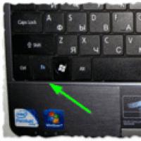 Ways how to make a screen on a laptop brighter or darker
 How to format a flash drive, disk protection
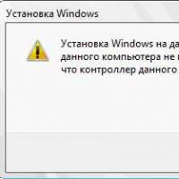 If installing Windows to this disc is not possible
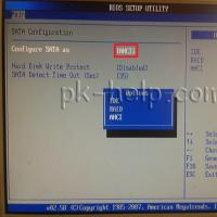 During installation of Windows "Make sure that the controller of this disc is included in the computer's BIOS menu.