What is equal to the exposure time in the CCD matrices. CCD. Physical principle of operation of the CCD. CCD matrix. Focal length and viewing angle
Solid state photovoltaic converters (TFEP) images are analogues of transmitting CRT.
TFEP began since 1970, with the so-called CCD and are formed on the basis of individual cells representing the Capacitors of the MDP or MOS structure. One of the plates of such an elementary capacitor is Metal film M, the second - semiconductor substrate P ( p.- or n.-Ronomials), dielectric d serves a semiconductor applied as a thin layer on the substrate P. as a substrate P silicon doped with acceptor ( p.-Type) or donor ( n.-Type) impurity, and as d - silicon oxide SiO. 2 (see Fig.8.8).
Fig. 8.8.Condenser MOS-Structure
Fig. 8.9.Moving charges under the action of the electric field
Fig. 8.10.The principle of operation of the three-phase CCD system
Fig. 8.11.Moving charges in a two-phase CCD system
When applying for a metal voltage electrode, a "pocket" or a potential pit is formed under it, in which the non-core carriers can "accumulate" (in our case), and the main carriers, holes will be repelled from M. on some distance from the surface The concentration of non-core carriers may turn out to be higher than the main concentration. Near the dielectric d in the substrate n occurs an inversion layer in which the type of conductivity changes to the opposite.
The charging package in the CCD can be administered by electrically or using light generation. With light generation of photovoltaic processes arising in silicon, will lead to the accumulation of non-core carriers in potential pits. The accumulated charge is proportional to the illumination and time of accumulation. The directional charge of the charge in the CCD is ensured by the location of MOS capacitors at such a close distance from each other, which their depleted areas overlap and potential wells are connected. At the same time, the movable charge of non-core carriers will accumulate in the place where the potential pit is deeper.
Let under the influence of the light accumulated charge under the electrode U. 1 (see Fig.8.9). If now on the adjacent electrode U. 2 Submit voltage U. 2 \u003e U. 1, then a different potential pit appears near, deeper ( U. 2 \u003e U. one). A region of the electric field and non-core carriers will arise between them (electrons) will drift (flow) into a deeper "pocket" (see Fig. 8.9). To exclude bidirectional in charge transmission, the sequence of electrodes combined into groups of 3 electrodes is used (see Fig. 8.10).
If, for example, accumulated charge under the electrode 4 and it is necessary to transfer it to the right, then a higher voltage is supplied to the right electrode 5 ( U. 2 \u003e U. 1) and the charge flows to it, etc.
Almost the entire totality of the electrodes is connected to the three tires:
I - 1, 4, 7, ...
II - 2, 5, 8, ...
III - 3, 6, 9, ...
In our case, the voltage "reception" ( U. 2) will be on the electrodes 2 and 5, but the electrode 2 is separated from the electrode 4, where the charge is stored, the electrode 3 (from which
U. 3 \u003d 0), so the flux to the left will not be.
The trinket operation of the CCD implies the presence of three electrodes (cells) to one element of the TV image, which reduces the useful area used by the light stream. To reduce the number of cells (electrodes) of the CCD, metal electrodes and a dielectric layer are formed by a stepped form (see Fig. 8.11). This allows, when the voltage pulses is supplied to electrodes, potential pits of different depths under its various sections. In a deeper pit, most charges from the neighboring cell flow.
With a two-phase CCD system, the number of electrodes (cells) in the matrix is \u200b\u200breduced by one third, which favorably affects the reading relief.
The CCC was first offered to use in computing technology as storage devices, shift registers. At the beginning of the chain, an injectionary diode was put in charge, and at the end of the chain - an output diode is usually n-P- or p-N-mOP transitions structures forming with the first and last electrodes (cells) of the CCD Field Transistors chains.
But soon it turned out that the CCD is very sensitive to light, and therefore they are better and more efficient to use as light reproduces, and not as storage devices.
If the CCD matrix is \u200b\u200bused as a photodetector, then the accumulation of charge under one or another electrode can be carried out by the optical method (injecting light). It can be said that the CCD matrices are essentially photosensitive analog shift registers. Today, the CCD is not used as storage devices (memory), but only as photodetectors. They are used in fax machines, scanners (CCD rules), in camera and video cameras (CCD matrix). Usually the so-called CCD chips are used in TV cameras.
We assumed that all 100% charges are transmitted to the neighboring pocket. However, in practice it has to be considered losses. One of the sources of losses is "traps" capable of capturing and hold some charges. These charges do not have time to flow into the nearby pocket, if the transfer rate is great.
The second reason is the flow mechanism itself. At the first moment, the transfer of charges occurs in a strong electric field - drift in E.. However, as charged charges, the field strength falls and the drift process fades, so the last portion moves due to diffusion, 100 times slower drift. Wait for the last portion - it means to reduce the speed. Draif gives more than 90% of the transfer. But it is the last percentages that are basic when determining losses.
Let the transmission coefficient of one transfer cycle equals k. \u003d 0.99, believing the number of cycles equal N. \u003d 100, we define the total transmission coefficient:
0,99 100 = 0,366
It becomes obvious that with a large number of items, even minor losses on one element are most important for the chain as a whole.
Therefore, the question of reducing the number of charges of charges in the CCD matrix is \u200b\u200bparticularly important. In this regard, the matrix of a two-phase CCD the charge transmission coefficient will be somewhat large than in a three-phase system.
In recent years, enthusiastic reviews dedicated to the next "technological miracle, designed to influence the future of digital photography, designed to influence the future of digital photography, are quite common in the near-computer (and not only) Press. . But what is characteristic of the only year of the initial excitement gradually goes to "no", and most of the manufacturers of digital photographic equipment instead of "advanced development" prefer to use proven solutions.
I would venture to assume that the reason for such a development of events is quite simple - it is enough to pay attention to the "brilliant simplicity" of one decision. In fact, the resolution of the matrix is \u200b\u200bnot enough? And let's pixels not columns and rows, but to have a diagonal lines, and then "turn" by the software "picture" by 45 degrees, here we will give the resolution at once! It does not matter that it increases the clarity of only strictly vertical and horizontal lines, and inclined and curves (of which the real image consists) remain unchanged. The main thing is that the effect is observed, it means that it can be loud about it.
Unfortunately, the modern user is "spoiled by megapixels." He is not good that every time the permission of the developers of the "classic" CCD matrices have to be solved the most complex task to ensure an acceptable dynamic range and sensitivity of the sensor. But the "solutions" like the transition with rectangular to the octalone form of pixels, an ordinary photographer seems quite understandable and reasonable, after all it is so affordable in advertising booklets ...
The purpose of this article is to try at the simplest level to explain, from which the quality of the image obtained at the output from the CCD matrix depends. At the same time, on the quality of the optics, it is completely calmly possible to abstractly, the appearance of the second one by the "Slir" costing less than $ 1,000 (Nikon D 70) allows you to hope that the further increase in the permission of sensors for chambers of an acceptable price category will not be limited to "soapy" lenses.
Inner photoeffect
Thus, the image generated by the lens falls on the CCD matrix, that is, the rays of light fall on the photosensitive surface of the PZD elements, whose task is to convert photon energy into an electric charge. It happens around as follows.
For a photon that fell on the CCD element, there are three options for the development of the event, it either "smits" from the surface, or will be absorbed in the thickness of the semiconductor (material of the matrix), or the "trips through" its "work area". Obviously, the developers need to create such a sensor, in which the losses from the "ricochet" and "striking the wavelet" would be minimized. The same photons that were absorbed by the matrix form a pair of electron-hole if interaction occurred with the atom of the semiconductor crystal grille, or only a photon (or hole), if the interaction was with donor atoms or acceptor impurities, and both of the listed phenomena are called inland photoeffect. Of course, the internal photoeffect work of the sensor is not limited to, it is necessary to maintain the chargers of charge "taken" in the semiconductor in a special storage, and then count them.
Element of the CCD matrix
In general, the design of the CCD element looks like this: a silicon substrate P - type is equipped with channels from a semiconductor N -type. Over the channels are created by polycrystalline silicon electrodes with an insulating layer of silicon oxide. After the electric potential is filled to such an electrode, in the donken zone under the channel N -typ is created potential Yama, the purpose of which is to store electrons. The photon penetrating silicon leads to the generation of an electron, which is attracted by a potential pit and remains in it. A larger number of photons (bright light) provides a greater charge of the pit. Then you need to consider the value of this charge, referred to phototokand strengthen it.
Reading photoconductors of PZD elements is carried out so-called sequential shift registersthat transform the lines of charges at the entrance to the exit pulse series. This series is an analog signal, which further enters the amplifier.
Thus, with the help of a register, you can convert into analog signal charges of the string from the PZD elements. In fact, a serial shift register in the CCD matrices is implemented using the same PZD elements combined into a string. The operation of such a device is based on the ability instruments with charge tie (This is what denotes the abbreviation of the CCD) to exchange charges of their potential pits. Exchange is carried out due to the presence of special transfer electrodes (TRANSFER GATE) located between adjacent PZD elements. When the elevated potential is applied to the nearest electrode, the charge "flows" under it from a potential pit. Between the CCD elements can be located from two to four transfer electrodes, the "phase" of the shear register, which may be called a two-phase, three-phase or four-phase depends on their quantity.
The supply of potentials to the electrodes of transfer is synchronized in such a way that the movement of charges of potential yams of all CCD elements of the register occurs simultaneously. And for one cycle of transfers of the CCD elements, as it were, "transmitted along the chain" charges from left to right (or right to left). Well, the resulting "extreme" CCD element gives his charge to the device located at the output of the register, that is the amplifier.
In general, the sequential shift register is a device with a parallel inlet and a sequential output. Therefore, after reading all charges from the register, it is possible to submit a new string to its input, then the following and thus form a continuous analog signal based on two-dimensional array of phototok. In turn, the input parallel stream for the sequential shift register (i.e., the rows of the two-dimensional array of phototoks) is ensured by a set of vertically oriented sequential shift registers, which is called parallel shift register, and the whole design is generally just a device called the CCD matrix.
"Vertical" sequential shear registers that are parallel, are called pZS-matrix columnsAnd their work is completely synchronized. The two-dimensional array of the PZS-matrix photocurrents simultaneously shifts down one line, and it only happens after the charges of the previous line from the "at the bottom" of the sequential shift register went to the amplifier. Before the release of the sequential register, parallel is forced to idle. Well, the CCD Matrix itself must be connected to the chip (or their set), feeding the potentials to the electrodes of both serial and parallel shift registers, as well as the synchronizing work of both registers. In addition, you need a clock generator.

Full frame matrix
This type of sensor is the simplest from a constructive point of view and is referred. full-frame CCD matrix (Full-Frame CCD - Matrix). In addition to the "strapping" chips, such a type of matrices also needs a mechanical gate, overlapping the light stream after exposure. Prior to the complete closure of the shutter, the reading of charges cannot be started - with the working cycle of the parallel register of the shift to the phototokok, each of its pixels will add extra electrons caused by photons on the open surface of the CCD matrix. This phenomenon is called "Blank" charge in a full-frame matrix(Full - Frame Matrix SMEAR).
In this way, frame reading speed This scheme is limited to the speed of both parallel and sequential shift registers. It is also obvious that it is necessary to overlap the light stream, which is running from the lens before the completion of the reading process, so interval between exposure It also depends on the read speed.
There is an improved variant of the full-frame matrix, in which the charges of the parallel register do not arrive at the sequential entry, and "stored" in the buffer parallel register. This register is located under the main parallel register of the shift, the photocurrents are trained in the buffer register and already come to the sequential shift register. The surface of the buffer register is covered with opaque (more often metallic) panel, and the whole system has been named matrix with frame buffering (FRAME - TRANSFER CCD).

Matrix with frame buffering
In this scheme, potential pits of the main parallel shift register "empty" are noticeably faster, since when transferring rows to the buffer, there is no need for each line to expect a complete cycle of the sequential register. Therefore, the interval between exposure is reduced, however, it also falls the reading speed to "travel" at twice the distance. Thus, the interval between exposure is reduced only for two frames, although the cost of the device due to the buffer register increases significantly. However, the most noticeable disadvantage of matrices with frame buffering is the extension "route" of phototokov, which negatively affects their preservation of their values. And in any case, the mechanical shutter should be activated between the frames, so it's not necessary to speak about a continuous video signal.
Matrix with columns buffering
Especially for video equipment was developed a new type of matrices, in which the interval between exposure was minimized not for a pair of frames, but for a continuous flow. Of course, to ensure this continuity it was necessary to provide a refusal to mechanical shutter.
In fact, this scheme, which received the name matrix with columns buffering(Interline CCD -Matrix), in something similar to systems with frame buffering, it also uses a buffer parallel shift register, the PZD elements of which are hidden under an opaque coating. However, this buffer is not located in a single block under the main parallel register, its columns are "shuffled" between the columns of the main register. As a result, a buffer column is located next to each column of the main register, and immediately after exposure, the photocurrents are moved not "from top to bottom", but "from left to right" (or "right to left") and in just one working cycle gets into a buffer register, entirely and Fully freeing potential pits for the next exposure.
The charges that fell into the buffer register as usual are read through a serial shift register, that is, "top down". Since the reset of phototoks into the buffer register occurs in just one cycle, even in the absence of a mechanical shutter, there is nothing similar to the "wrapping" of the charge in the full-frame matrix. But the exposure time for each frame in most cases by duration corresponds to the interval spent on the full reading of the buffer parallel register. Thanks to all this, it is possible to create a video signal with a high frequency of personnel, at least 30 sides second.

Matrix with columns buffering
Often in the domestic literature, the matrix with buffering columns is mistakenly called "interlaced". It is probably caused by the fact that the English names "Interline" (lines buffering) and "Interlaced" (interlaced) sounds very similar. In fact, when reading for one tact of all lines, you can talk about the matrix with progressive scan (PROGRESSIVE SCAN), and when odd lines are read for the first beat, and for the second (or vice versa), we are talking about matrix with interlaced scan(Interlace Scan).
Although photocurrents of the main parallel shift register immediately fall into the buffer register, which is not subjected to "photonic bombardment", "Molding" charge in matrices with columns buffering (SMEAR) also occurs. It is caused by a partial flow of electrons from the potential pit of the "photosensitive" CCD element to the potential pit of the "buffer", especially often this happens with close to the maximum charge levels when the pixel illumination is very high. As a result, a light strip stretches from this bright point in the picture up and down from this bright point. To combat this unpleasant effect, when designing a "photosensitive" sensor and buffer columns are located at a greater distance from each other. Of course, it complicates the exchange of charge, and also increases the time interval of this operation, but the harm that makes the image of "folding", does not leave the selection developers.
As mentioned earlier, it is necessary to ensure the video signal to ensure that the sensor does not require the overlap of the light stream between exposures, since the mechanical shutter in such working conditions (about 30 triggers per second) can quickly fail. Fortunately, thanks to the buffer lines there is an opportunity to implement electronic shutterwhich, firstly, allows you to do without a mechanical shutter if necessary, and secondly, provides supermarines (up to 1/10000 pieces) excerpt values, especially critical for shooting rapid processes (sport, nature IT.D.). However, the electronic shutter also requires that the matrix has a system for removing the excess charge of a potential pit, however, everything will be described in order.
For everything you have to pay, and for the ability to form a video signal, too. The shift buffer registers "eat" a significant part of the matrix area, as a result of each pixel only gets 30% of the photosensitive area from its total surface, while the pixel is a full-frame matrix this area is 70%. That is why in most modern CCDs_matics on top of each pixel is located microlinza. Such a simplest optical device covers most of the PZS-element area and collects all the fraction of photons falling on this part into a concentrated light stream, which, in turn, is directed to a fairly compact photosensitive pixel region.

Microlinze
Since using microlins, it is possible to register the light stream falling on the sensor to the sensor much more efficiently, with time these devices began to supply not only systems with columns buffering, but also full-frame matrices. However, microlynes should not be called a "solution without flaws".
Being an optical device, microlynes in one way or another distort the recorded image is most often expressed in loss of clarity at the smallest parts of the frame, their edges become slightly blurred. On the other hand, such a unwitting image is not always undesirable - in some cases, the image generated by the lens contains lines, the size and frequency of the placement of which are close to the size of the CCD element and the interpixel distance of the matrix. In this case, the frame is often observed study (Aliasing) - Possing a pixel of a certain color, regardless of whether it is covered with a part of an image or only part of it. As a result, the object of the object in the picture is obtained by torn, with gear edges. To solve this problem in cameras with matrices without microlysis, an expensive specrah Protection Filter (Anti -AliaSing Filter), and the sensor with microlines in such a filter does not need. However, in any case, it has to pay for some decrease in the sensor resolution.
If the object of shooting is not high enough, it is recommended to open the diaphragm as much as possible. However, the percentage of rays falling on the surface of the matrix at a steep angle increases dramatically. Microlinzes are chipped by a significant proportion of such rays, therefore the efficiency of light absorption by the matrix (that, for which they opened the diaphragm) is greatly reduced. Although it should be noted that the rays falling at a steep angle are also a source probleming in silicon of a single pixel, a photon with a large wavelength, having a high penetrating ability, can absorb the material of another matrix element, which will eventually lead to a distortion of the image. To solve this problem, the matrix surface is covered with an opaque (for example, metal) "lattice", in the cuts of which only the photosensitive zones of pixels remain.
Historically, the full-frame sensors are used mainly in the studio technician, and the matrixes with the buffering of columns are amateur. In professional cameras there are sensors of both types.
In the classic CCD element scheme, which uses polycrystalline silicon electrodes, sensitivity is limited due to partial light scattering the surface of the electrode. Therefore, when shooting in specific conditions, requiring increased sensitivity in blue and ultraviolet areas of the spectrum, the matrices with reverse illumination are used (Back -illuminated Matrix). In sensors of this type, the recorded light falls on the substrate, and in order to ensure the required internal photoeffect of the substrate grinding to a thickness of 10-15 micrometers. This stage of processing greatly retained the cost of the matrix, in addition, the devices were obtained very fragile and demanded increased caution when assembling and operation.

Back-up matrix
Obviously, when using light filters that weaken the light stream, all expensive surgery to increase sensitivity lose meaning, so the matrix with inverse illumination are used for the most part in the astronomical photography.
Sensitivity
One of the most important characteristics of the recording device, whether it is a photography or CCD matrix, is sensitivity - The ability to react to optical radiation in a certain way. The higher the sensitivity, the smaller the amount of light is required to react the recorder device. Different quantities (DIN, ASA) were used to designate sensitivity, but ultimately practiced practices denote this parameter in ISO (International Standards Organization- International Standards Organization).
For a separate CCD element, a charge generation should be understood. It is obvious that the sensitivity of the CCD matrix is \u200b\u200bconsisted of the sensitivity of all its pixels and as a whole depends on the two parameters.
First parameter - integral sensitivity, which is the ratio of the magnitude of the photocurrent (in milliamperes) to light flow (in lumens) from the radiation source, the spectral composition of which corresponds to a tungsten incandescent lamp. This parameter allows you to estimate the sensitivity of the sensor as a whole.
The second parameter - monochromatic sensitivity, That is, the ratio of the magnitude of the photocurrent (in milliampeurs) to the magnitude of the radiation light energy (in milli andlectronvolts) corresponding to a certain wavelength. A set of all the values \u200b\u200bof monochromatic sensitivity for the part of the spectrum of interest is spectral sensitivity - The dependence of sensitivity from the light wavelength. Thus, the spectral sensitivity shows the capabilities of the sensor to register shades of a certain color.
It is clear that the units of measurement as integral and monochrome sensitivity differ from the designations popular in photographic engineering. That is why manufacturers of digital photographic equipment in product characteristics indicate equivalent sensitivity CCD matrices in ISO units. And in order to determine the equivalent sensitivity, the manufacturer is enough to know the illumination of the shooting object, aperture and shutter speed, and use a pair of formulas. According to the first, the exposition number is calculated as Log 2 (L * S / C), where L is illumination, S is sensitivity, and C is an exposure meter constant. The second formula defines an exposure number to 2 * log 2 k - log 2 t., Where k is a diaphragm number, and T -put. It is easy to remove the formula that allows L, C, K and T to calculate, which is equal to s.
The sensitivity of the matrix is \u200b\u200ban integral value depending on the sensitivity of each CCD element. Well, the sensitivity of the pixel matrix depends, firstly, from "the photons substituted under the rain" square of photosensitive region (Fill Factor), and secondly, from quantum efficiency (Quantum Efficiency), that is, the rating of the number of registered electrons to the number of photon sensor dropped on the surface.
In turn, a number of other parameters affect quantum efficiency. First, it is reflection coefficient - The value that displays the share of those photons that "twisted" from the surface of the sensor. As an increase in the reflection coefficient, the proportion of photons participating in the inner photoeffect decreases.
The photons not reflected from the surface of the sensor will absorb, forming charge carriers, but some of them will be "stuck" at the surface, and the part will penetrate too deep into the material of the CCD element. Obviously, in both cases they will not take any participation in the process of forming a photocurrent. "Penetrating ability" of photons in a semiconductor, referred to the absorption coefficientDepends on both the semiconductor material and the wavelength of the incident light - "long-wave" particles penetrate much deeper "shortwave". Working out the CCD element is necessary for photons with a wavelength corresponding to the visible radiation, to achieve such a absorption coefficient so that the internal photoelectric effect occurs near the potential pit, thereby increasing the chance for an electron to get into it.
Often, instead of quantum efficiency, the term is used "Quantum output" (Quantum yield), but in reality this parameter displays the number of charge carriers released when absorbing one photon. Of course, with an internal photoeffect, the bulk of charge carriers still falls into the potential pzs-element yam, but a certain part of electrons (or holes) avoids "traps". In the numerator of the formula describing the quantum efficiency, it is exactly the number of charge carriers that hit the potential pit.
An important characteristic of the CCD matrix is sensitivity threshold - The parameter of the recorder of the device, which characterizes the minimum value of the light signal, which can be registered. The smaller this signal is the higher the sensitivity threshold. The main factor limiting the sensitivity threshold is dark current (Dark Current). It is a consequence of thermoelectronic emissions and occurs in the CCD element when the potential for the electrode is submitted, under which a potential pit is formed. "Dark" is called this current because it consists of electrons that have fallen into a pit with the complete absence of a light flux. If the light stream is weak, then the magnitude of the photocurrent is close, and sometimes less than the value of the dark current.
There is a dependence of the dark current from the temperature of the sensor, when the matrix is \u200b\u200bheated by 9 degrees Celsius, its dark current increases twice. For cooling the matrix are used different heat sink systems (cooling). In the field chambers, the mass-darling characteristics of which strongly limit the use of cooling systems, sometimes a metal chamber body is used as a heat exchanger. In the studio technique, there are practically no restrictions on mass and dimensions, moreover, a sufficiently high power consumption of the cooling system, which, in turn, are divided into passive and active ones are allowed.
Passive cooling systems We only provide a "reset" of excess heat of the cooled device into the atmosphere. In this case, the cooling system plays the role of maximum heat conductor, providing more efficient dispersion. Obviously, the temperature of the cooled device cannot become lower than the ambient temperature in which the main lack of passive systems is.
The simplest example of a passive heat exchange system is radiator (Heatsink) made of material with good thermal conductivity, most often - from metal. The surface in contact with the atmosphere has a form that provides as many scattering area as possible. Generally accepted maximum scattering area possess needle radiators, in shape resembling "hedgehog", covered with scattering heat "needles". Often for the forcing heat exchange, the surface of the radiator is blown away micoventio- Similar devices called coolers (Cooler, from the word Cool-cooling), cool the processor in personal computers. Based on the fact that the michenetizer consumes electricity to use its systems called "active"., That is completely wrong, since the coolers cannot cool the device to a temperature of less than atmospheric. At high ambient air temperature (40WORDS and above), the effectiveness of passive cooling systems is beginning to fall.
Active cooling systems Due to electrical or chemical processes, provide the device temperatures below the ambient air. In fact, the active systems "produce cold", however, it is allocated to the atmosphere both the heat of the cooled device and the heat of the cooling system. A classic example of the active cooler is the usual refrigerator. However, despite the rather high efficiency, its mass-darling characteristics are unacceptable even for studio photographic equipment. Therefore, its active cooling is ensured. peltier systems whose work is based on the use of the effect of the same name, when in the presence of potential difference at the ends of two conductors made from different materials, at the junction of these conductors (depending on the polarity of the voltage) will be released, or the heat energy is absorbed. The reason for the acceleration or slowing down electrons due to the internal contact difference potential potentials of the conductors.
When using a combination of N-type semiconductors and p-type, in which heat-absorption is made due to the interaction of electrons and "holes", the maximum heat-conducting effect occurs. To enhance it, you can apply a cascade association of Peltier elements, and because it occurs both the absorption of heat and the selection, the elements must be combined so that one side of the cooler is "hot", and the other "cold". As a result of cascading combination, the temperature of the "hot" side of the most remote from the matrix of the Peltier element is significantly higher than that of the ambient air, and its heat dissipates in the atmosphere using passive devices, that is, radiators and coolers.
Using Peltier Effect The active cooling systems can lower the temperature of the sensor up to zero of degrees, radically reducing the level of the dark current. However, excessive cooling of the CCD matrix threatens with the loss of moisture condensate from the ambient air and the short circuit of electronics. And in some cases, the limiting temperature difference between the cooled and photosensitive planes of the matrix can lead to its unacceptable deformation.
However, neither radiators or coolers nor the elements of Peltier are applicable to field chambers, limited by weight and dimensions. Instead, this technique uses a method based on so-called black pixelch (Dark Reference Pixels). These pixels are coated with an opaque material columns and strings along the edges of the matrix. Averaged value for all photoclies of black pixels is considered dark current level. Obviously, under different operating conditions (ambient temperature and camera itself, batteries current, etc.), the dark current level will be different. When using it as a "point of reference" for each pixel, that is, the value of its value from the photo stream can be determined which one charge is created by the photons falling on the CCD element.
Suppressing in one way or another in the dark current, you should remember the other factor limiting the sensitivity threshold. It is thermal noise (THERMAL NOISE), created even in the absence of potential on electrodes with only the chaotic movement of electrons by the CCD element. Exposures of high duration lead to gradual accumulation of wandering electrons in a potential pit, which distorts the true value of the photocurrent. And the "longer" excerpt, the more "lost" in the email of electrons.
As you know, the photosensitivity of the film within the same cassette remains constant, in other words, it cannot be changed from the frame to the frame. But the digital camera allows for each snapshot to set the most optimal value of equivalent sensitivity. This is achieved by enhancing the video signal emanating from the matrix - in something such a procedure called "Increased equivalent sensitivity"Reminds the rotation of the player volume regulator.
Thus, with weak lighting, the user comes to a dilemma, or increase the equivalent sensitivity, or increase the shutter speed. At the same time, in both cases, it does not avoid damage to the frame of fixed distribution noise. True, experience shows that with a "long" shutter speed, the snapshot does not deteriorate as much as when the matrix signal is gained. However, the big duration of exposure threatens another problem - the user can "grasp" frame. Therefore, if you want to use a frequent shooting in the room, then it should choose a camera with a high lens light, as well as a powerful and "intelligent" flash.
Dynamic range
From the matrix, the ability to register light both in the bright sun and with low room lighting is required. Therefore, potential matrician pits should be very capacious, as well as be able to keep the minimum amount of electrons with weak light, so and accommodate a large charge, obtained by hitting a powerful lighting sensor. Yes, and an image formable by the lens often consists of both brightly illuminated areas and from deep shadows, and the sensor should be able to register all their shades.
The ability of the sensor to form a good picture with different illumination and high contrast is determined by the parameter "Dynamic range"characterizing the ability of the matrix in the image projected onto its registering surface, the darkest tones from the brightest. With the expansion of the dynamic range, the number of shades of the picture will increase, and the transitions between them will most correspond to the image formable by the lens.

Effect of dynamic range on frame quality (A - wide dynamic range, b - narrow dynamic range)
The characteristic describing the ability of the CCD element to accumulate a certain value is called "Potential Poam Depth" (Well Depth), and it is precisely the dynamic range of the matrix that depends. Of course, when shooting under conditions of weak lighting, the sensitivity threshold also affects the dynamic range, which, in turn, is determined by the value of the dark current.
It is obvious that the losses of electrons constituting the photocurrent occur not only in the process of accumulating the charge of a potential pit, but also during its transportation to the output of the matrix. These losses are caused by the drift of electrons, "torn" from the main charge when it is flowing for the next electrode of transfer. The smaller the number of "broken" electrons, the higher charge transfer efficiency CHARGE TRANSFER EFFICIENCY). This parameter is measured as a percentage and shows the share of charge, preserved when the "crossing" between the CCD elements.
The effect of transfer efficiency can be demonstrated on the following example. If the value of this parameter is 98% for the matrix 1024 x 1024, then it is necessary to determine the value of a central pixel photocurrent at the output of the matrix; it is necessary to build 1024 to 1024 (the amount of "crossing" between pixels) and multiply by 100 (interest ). The result is completely unsatisfactory - some 0.0000001% will remain from the initial charge. It is obvious that with the increase in permission, the requirements for transfer efficiency becomes even more hard, since the number of "crossing" increases. In addition, the reading rate of the frame falls, because the increase in the transfer rate (to compensate for the increased resolution) leads to an unacceptable increase in the number of "broken" electrons.
In order to achieve acceptable frame reading rates at high charge transfer efficiency when designing a CCD matrix, planned "Blind" placement of potential pits. Due to this, the electrons are not so actively "sticking" to the transfer electrodes, and it is for a "deep running" of a potential pit in the design of the CCD element, an N-channel is administered.
Returning to the above example: if in this matrix 1024 x 1024 the charge transfer efficiency will be 99.999%, then 98.98% of its initial value will remain at the output of the sensor from the sensor from the central charge. If a higher resolution matrix is \u200b\u200bbeing developed, then the efficiency of charge transfer is 99.9999%.
Blooming
In cases where the internal photoeff leads to an excess number of electrons exceeding the depth of the potential pit, the charge of the CCD element begins to "spread" along the neighboring pixels. In the pictures, this phenomenon is called "Bluming" (From English Blooming - erosion), it is displayed as white spots and the correct shape, and the more excess electrons, the larger the stains.
Blooney suppression is carried out by system electronic drainage (Overflow Drain), the main task of which is the removal of excess electrons from the potential well. The most famous options vertical drainage (Vertical Overflow Drain, Vod) and side drainage (Lateral Overflow Drain, Vod).
The system with vertical drainage on the matrix substrate is given potential, the value of which is selected so that when overflowing the depth of the potential pit, excess electrons flowed out of it on the substrate and dissipated there. The disadvantage of such an embodiment is to reduce the depth of the potential pit and, accordingly, the narrowing of the dynamic range of the CCD element. It is also obvious that this system is not applicable in matrices with inverse illumination.

Vertical electronic drainage
The system with side drainage uses electrodes that prevent the penetration of electron potential pits into "drainage grooves", from which the excess charge is scattered. The potential on these electrodes is selected in accordance with the barrier of the overflow of the potential well, while its depth does not change. However, due to the drainage electrodes, the photosensitive area of \u200b\u200bthe CCD element is reduced, so microlens have to use.

Side electronic drainage
Of course, the need to add to the sensor drainage devices complicates its design, but the distortion of the frame made by blooming cannot be ignored. Yes, and the electronic shutter cannot be implemented without drainage, it plays the role of "curtains" at ultrashort excerpts, the duration of which is less than the interval spent on the transfer of charge from the main parallel shift register to the buffer parallel register. "Shutter", that is, drainage, prevents the buffer pipples of those electrons into the pit, which were formed in "photosensitive" pixels after the specified (and very short) exposure time passed.
"Gulp" pixels
Due to technological errors in some CCD elements, even the shortest excerpt leads to avalanche-like accumulation of electrons in a potential pit. In the picture such pixels, referred to "Gulp" (Stuck Pixels), very much differ from the surrounding points both in color and in brightness, and, in contrast to the noise of fixed distribution, they appear at any excerpt and regardless of the heating of the matrix.
Removing the pixels of pixels is carried out through the built-in camera software, which ensures the search for defective PZD elements and memorizing their "coordinates" in non-volatile memory. When the image is generated, the value of defective pixels is not taken into the calculation, they are replaced by the interpolated value of adjacent points. To determine the defectiveness of the pixel during the search process, its charge is compared with the reference value, which is also stored in the non-volatile memory of the camera.
The size of the matrix diagonally
Sometimes in a number of other parameters of any digital camera indicates the size of the CCD matrix diagonally (most often in inches). First of all, this value is associated with the characteristics of the lens, the higher the size of the sensor, the larrhery should be an image formable by optics. So that this image completely covers the registering surface of the matrix, the size of the optical elements has to be increased. If this does not do and the "picture" created by the lens will be less sensor, the peripheral areas of the matrix will be unclaimed. However, in some cases, the camera manufacturers did not indicate that in their models a certain proportion of megapixels was "not deed."
But in digital "mirrors" created on the basis of 35-miliemeter techniques, there is almost always a reverse situation - an image formable by the lens, overlaps the photosensitive area of \u200b\u200bthe matrix. It is caused by the fact that the sensors with the dimensions of the frame 35-Milimetrone film are too expensive, but leads to the fact that a part of the image formable by the lens turns out to be literally the word "for the scenes". As a result, the characteristic of the lens is shifted to the "long-focus" area. Therefore, when choosing interchangeable optics for a digital "Mirrors" should be considered focal length increase coefficient - As a rule, it is about 1.5. For example, when installing a 30-70mm vario setting, its operating range will be 42-105mm.
The mentioned coefficient has both positive and negative influence. In particular, the shooting is complicated with a large corner of the coverage, requiring short-focus lenses. Optics with a focal length of 18mm and less is very expensive, and in the digital "srink" it turns into trivial 27mm. However, long-phocus lenses are also very expensive, and with a large focal length, as a rule, the relative hole is reduced. But an inexpensive 200-millimeter lens with a coefficient of 1.5 turns into a 300-millimeter, while the "real" 300-millimeter optics of a diaphragm of the order f / 5.6, in the 200-mm lights above, F / 4.5.
In addition, such aberrations are characteristic of any lens as the curvativity of the field and distortion, expressed in the blurry and curvature of the image in the regional regions of the frame. If the dimensions of the matrix are less than the size of the image-generated image, "problem areas" will simply not be registered with the sensor.
It should be noted that the sensitivity of the matrix is \u200b\u200bassociated with the dimensions of its registering area. The extensive photosensitive area of \u200b\u200beach element, the greater the light falls on it and the more often the inner photoeff is happening, thus, the sensitivity of the entire sensor increases. In addition, the pixel of large dimensions allows you to create a potential "enhanced capacity" a pit, which has a positive effect on the latitude of the dynamic range. A visual example of digital "mirrors", comparable in dimensions with a frame of a 35mm film. These sensors traditionally differ in the sensitivity of the order ISO 6400 (!), And the dynamic range requires ADC with a bit of 10-12-bit.
At the same time, the matrix of amateur chambers have a dynamic range for which there is enough 8-10-bit ADCs, and sensitivity rarely exceeds ISO 800. The reason for the design of this technique. The fact is that Sony company has very few competitors in terms of the production of small-sized (1/3, 1/2 and 2/3 inches diagonally) sensors for amateur equipment, and it was caused by a competent approach to the development of a model range of matrices. When developing the next generation of matrices with permission to "per megapixel more", almost complete compatibility with previous models of sensors was provided, and both in size and the interface. Accordingly, the camera designers did not have "from scratch" to develop the lens and "electronic filling" of the chamber.
However, with increasing permission, the buffer parallel shift register captures an increasing share of the sensor area, as a result of the photosensitive region, and the "capacity" of the potential wells are reduced.

Reducing the photosensitive region of the CCD matrix with an increase in permission.
Therefore, for each "n +1 megapixel", the painstaking work of developers are linked, unfortunately, not always successful.
Analog-Digital Converter
The video signal that has passed through the amplifier must be translated into the digital format clear microprocessor. For this, used analog-Digital Converter, ADC (Analog to Digital Convertor, ADC) - a device that converts analog signal into a sequence of numbers. Its main characteristic is bigness, that is, the number of recognizable and encoded discrete signal levels. To calculate the number of levels, it is enough to build a two to the degree of bit. For example, the "bit 8 bits" indicates that the converter is able to determine 2 to the eighth degree of signal levels and display them in the form of 256 different values.
With a big discharge, the ADC can (theoretically) achieve greater color depths (Color depth), that is, color processing discharge, describing the maximum number of color shades that can be reproduced. The color depth is usually expressed in bits, and the number of shades is calculated in the same way as the number of signal levels of the ADC. For example, with a 24-bit color depth, you can get 16777216 shades of color.
In reality, the depth of color for files in JPEG formats or TIFF, which are used by the computer for processing and storing images, is limited to 24 bits (8 bits per color channel - blue, red and green). Therefore, sometimes used ADCs with a bit of 10, 12, and even 16 bits (that is, color depth 30, 36 and 48 bits) can be mistakenly calculated "redundant". However, the dynamic range of the matrix of some models of digital photographic equipment is quite wide, and if the camera is equipped with a frame for saving a frame in a non-standard format (30-48 bits), then with further computer processing it is possible to use "extra" bits. As is known, errors in the calculation of the exposition in the frequency of manifestation are inferior only to the inaccuracies of focusing. And therefore the ability to compensate for such errors using the "lower" (in the case of undershits) or the "top" (when overtaking) the bit turns out to be quite by the way. Well, if the exposure is designed without errors, then "compress" without distortion 30-48 bits in standard 24 is not a particularly difficult task.
It is obvious that the dynamic range of the CCD matrix should be the basis for increasing the BTP's discharge, since with a narrow dynamic range of ADCs with 10-12 bits to the channel simply nothing to recognize. And often it is impossible to be called differently than the advertising trick of the mention of the "36-bit" and even "48-bit" color of the modest "soap" with a matrix in half a diagonal, because even 30-bit color requires at least a sensor with a diagonal 2 / 3 inches.
For the first time, the principle of the CCD with the idea to maintain and then read the electronic charges was developed by two engineers of the Bell corporation in the late 60s during the search for new types of memory for computers capable of replacing memory on ferrite rings (yes - yes, there was such a memory). This idea turned out to be unpromising, but the ability of silicon to respond to a visible radiation spectrum was noticed and the thought to use this principle for image processing was developed.
Let's start with the decryption of the term.
The abbreviation of the CCD means "Instruments with Charging Communication" - this term was formed from English "CHARGE-COUPLED DEVICES" (CCD).
This type of instrument currently has a very wide range of applications in a wide variety of optoelectronic devices for registration of the image. In everyday life, these are digital cameras, camcorders, various scanners.
What distinguishes the CCD receiver from a conventional semiconductor photodium having a photosensitive area and two electrical contacts for removing an electrical signal?
Firstly , such photosensitive sites (often called pixels - elements receiving light and transform it into electrical charges) in the CCD receiver a lot, from several thousand to several hundred thousand and even several million. The dimensions of individual pixels are the same and can be from units to tens of microns. The pixels can be built in one row - then the receiver is called the PZS-line, or with even rows of filling the surface area - then the receiver is called the CCD matrix.
Right-racing light-receiving elements (blue rectangles) in the CCD line and the CCD matrix.
Secondly , in the CCD receiver, externally similar to the usual chip, there is no huge number of electrical contacts for outputting electrical signals that seem to have to go from each light-receiving element. But the electronic circuit is connected to the CCD receiver, which allows you to remove an electrical signal from each photosensitive element, proportional to its illumination.
The Action CCD can be described as follows: Each photosensitive element - pixel - works like a piggy bank for electrons. Electrons arise in pixels under the action of light that came from the source. During the specified time interval, each pixel is gradually filled with electrons in proportion to the number of light in it, like a bucket put on the street during the rain. At the end of this time, electrical charges accumulated by each pixel are passed to the "output" of the device and are measured. All this is possible due to a certain structure of the crystal, where the photosensitive elements and the electrical control circuit are placed.
Almost exactly the CCD matrix also works. After exposure (illumination of the projected image), the electronic control circuit of the instrument gives it a complex set of pulse stresses, which begin to shift the columns with electrons accumulated in pixels to the edge of the matrix, where there is a similar measuring CCD register, charges in which are shifted already in the perpendicular direction and fall On the measuring element, creating signals in it proportional to individual charges. Thus, for each subsequent point in time, we can get the value of the accumulated charge and figure out what pixel on the matrix (row number and number of the column) it corresponds.
Brief about the physics of the process.
To begin with, we note that the CCD belongs to the products of the so-called functional electronics, they cannot be submitted as a set of individual radio elements - transistors, resistance and capacitors. The basis of work is the principle of charge. The principle of charge uses two positions known from electrostatics:
- the charges of the same name are repelled
- the charges strive to settle down where their potential energy is minimal. Those. Roughly - "Fish is looking for where deeper."
First, imagine a MOS capacitor (MOP - a reduction from the words of the metal-oxide semiconductor). This is what remains from the MOS transistor, if you remove the stock and source from it, that is, the electrode separated from the silicon layer of dielectric. For certainty, we assume that the semiconductor is p-type, i.e., the concentration of holes in equilibrium conditions has a lot (several orders) more than electrons. In the electrophysics "hole" call the charge, reverse charge of the electron, i.e. Positive charge.
What will happen if on such an electrode (it is called a shutter) to submit a positive potential? The electric field created by the shutter, penetrating into silicon through the dielectric, repels moving holes; There is a depleted area - some of the scope of silicon free from the main carriers. In parameters of semiconductor substrates typical of the CCD, the depth of this region is about 5 microns. On the contrary, the electrons arising here under the influence of light will attract the shutter and will accumulate on the border of the oxide-silicon section directly under the shutter, that is, they fall into the potential pit (Fig. 1).

Fig. one
The formation of a potential pit when the voltage is applied to the dam
In this case, the electrons are partially neutralized by the electric field created in the semiconductor by the shutter, and in the end can fully compensate for it, so that the entire electric field will fall only on the dielectric, and everything will return to its original state - by the exception that At the interface, a thin layer of electrons is formed.
Let now be near the shutter there is another shutter, and the positive potential is also filed on it, and more than the first (Fig. 2). If only the shutters are located close enough, their potential pits are combined, and electrons that are in one potential pit are moved to the neighboring, if it is "deeper." 
Fig. 2.
The overlapping of the potential holes of two closely arranged shutters. The charge flows into the place where the potential pit is deeper.
Now it should be clear that if we have a chain of shutters, then you can, feeding on them the corresponding control stresses, transfer the localized charging package along such a structure. The wonderful property of the CCD is the property of self-scanning - it is that for the control of the chain of the shutters of any length is just three clock tires. (The term tire in electronics is an electric current conductor connecting the same type of elements, clock bus - conductors for which the voltage displaced in phase is transmitted.) Indeed, for the transfer of charge packets it is necessary and sufficiently three electrodes: one transmitting, one receiving and one insulating, separating pair. receiving and transmitting each other, and the same electrodes of such triples can be connected to each other into a single clock tire, requiring only one external output (Fig. 3).

Fig. 3.
The simplest three-phase CCD register.
The charge in every potential pit is different.
This is the simplest three-phase register of the shift on the CCD. The clock charts of such a register are shown in Fig. four.

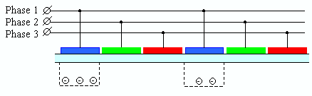
Fig. four
The clock charts of control of the three-phase register are three meander shifted by 120 degrees.
When changing the potentials, the movement of charges.
It can be seen that for its normal operation at each moment of time, at least one clock tire must be present high potential, and at least one - low potential (barrier potential). With increasing potential on one bus and lowering it on another (previous), the simultaneous transmission of all charged packets under the adjacent shutters, and for the full cycle (one clock on each phase bus) takes place (shift) of charge packets to one register element.
For the localization of charge packets in the transverse direction, the so-called stop channels are formed - narrow strips with an increased concentration of the main alloying impurities going along the transfer channel (Fig. 5).

Fig. five.
View of the Register "Top".
Transfer channel in the lateral direction is limited to stop channels.
The fact is that from the concentration of the alloying impurity depends, with what specifically, the tension on the gate under it is formed a depleted area (this parameter is nothing but a threshold voltage of the MOS structure). Of the intuitive considerations, it is clear that the larger the concentration of the impurity, that is, the more holes in the semiconductor, the more difficult to drive into the depth, that is, the higher the threshold voltage or, at one voltage, the lower the potential in the potential pit.
Problems
If, in the production of digital devices, the variation of the parameters on the plate can reach several times without noticeable effect on the parameters of the instruments obtained (since the work comes with discrete voltage levels), then in the CCD change, say, the concentration of the alloying impurity is 10% already marked in the image. The size of the crystal, and the impossibility of reservation, as in the bis of memory, adds their own problems, so the defective areas lead to the disrepair of the entire crystal.
Outcome
Different pixels of the CCD matrix technologically have different sensitivity to the light and this difference must be adjusted.
In the digital CMA, this correction is called the Auto Gain Control system (AGC)
How the AGC system works
For ease of consideration, we will not take something specific. Suppose that at the output of the ADC node of the CCD has some potential levels. Suppose that 60 is the average level of white.


- For each pixel, the CCD line is read when illuminated by its reference white light (and in more serious devices - and reading the "black level").
- The value is compared with a reference level (for example, average).
- The difference between the output value and the reference level is remembered for each pixel.
- In the future, when scanning, this difference is compensated for each pixel.
The AGC system initialization is performed every time the scanner system is initialized. Probably, you noticed that when the car is turned on, after some time, the scanner carriage begins to perform progressive movements (choking u h / b stripes). This is the initialization process of the AGC system. The system also takes into account the state of the lamp (aging).
Also, you probably paid attention that small MFPs equipped with a color scanner "light up the lamp" three colors in turn: red, blue and green. Then only the backlight of the original is ignited by white. This is done for better sensitivity correction of the matrix separately via RGB channels.
Test halftone Shading Test) Allows you to initiate this procedure at the request of the engineer and bring the correction values \u200b\u200bfor real conditions.
Let's try to consider all this on the real, "combat" car. We will take a well-known and popular apparatus SAMSUNG SCX-4521 (Xerox PE 220).
It should be noted that in our case the CCD becomes CIS (Contact Image Sensor), but the essence of what is happening in the root does not change. It is simply used as a light source of LEDs.
So:
The image signal from CIS has a level of about 1.2 V and enters the ADC section (SATS) of the controller of the apparatus (SATSP). After the SATSP, the analog CIS signal will be converted to an 8-bit digital signal.
The image processor in the SATSP primarily uses the tone correction function, and then the gamma correction function. After that, the data is fed to various modules in accordance with the mode of operation. In Text mode, these images enroll on the LAT module, in Photo mode, the image data is received by the "Error Diffusion" module, in PC-SCAN mode, the image data arrive directly to a personal computer via DMA access.
Before testing, put several clean sheets of white paper on the exposure glass. It goes without saying that optics, b / b band and generally the scanner node from the inside should be pre-licked "
- Choose in Tech Mode
- Press the ENTER button to scan the image.
- After scanning will be printed "CIS SHADING PROFILE" (CIS Halfone Profile). An example of such a sheet is given below. It is not necessary that it should be a copy of your result, but close in the image.
- If the printed image is very different from the image shown in the figure, then CIS is faulty. Please note - at the bottom of the report sheet written "Results: OK". This means that the system of serious complaints to the CIS module has no. Otherwise, the results of errors will be given.
Example Printing Profile:

Good luck to you!!
As a basis, materials of articles and lectures of St. Petersburg State University (LSU), Spbet (LETI) and AXL are taken as a basis. Thank you.
Material prepared by V. Shelenberg
After reading the previous part, our reader could have the impression that the CCD matrix was a kind of "black box", an outstanding "electronic negative" after a light image created by the lens created by the lens, and that the picture the picture is also affected exclusively Size sensor.
The same point of view is adhered to sellers of digital photographic equipment, gently, but persistently pushing the potential buyer to acquire a model with as much as possible a large-sized matrix, even if there is no objective reasons for such a purchase. More often as a "bait" for the client, various kinds of "unique developments" are performing when creating a matrix, which, oddly enough, do not apply to anyone from other manufacturers.
A beginner photographer is difficult to distinguish promotional promises from truly efficient engineering finds. This article will attempt to "separate the grains from the whores", however, for a start, you must familiarize yourself with the basic definitions of digital photography.
As a photon becomes an electron
In charge charges, the photon transformation into an electron is made as a result of an internal photo effect: absorption of the light quantum with a semiconductor crystal grille with the release of charge carriers. It can be either a pair of "electron + hole", or a single charge carrier - the latter occurs when using donor or acceptor impurities in the semiconductor. Obviously, the formed charge carriers must somehow save before reading.
For this, the main Material of the CCD matrix is \u200b\u200ba silicon substrate P-type - equipped with channels from the N-type semiconductor, over which the electrodes are made of polycrystalline silicon. After the electric potential, a potential pit is created under the electrode of the electrical potential in the depleted zone under the N-type channel, the appointment of which is to store the charge, "mined" by means of an internal photo effect. The more the photons fall on the CCD element (pixel) and turn into electrons, the higher the charge accumulated by the pit.
Element of the CCD matrix
Pixel CCD-Matrix section
To get an "electronic negative", it is necessary to consider the charge of each potential pit of the matrix. This charge received the name of the photo stream, its value is quite small and after reading requires compulsory gain.
The charge reading is made by the device connected to the most extreme row of the matrix, which is called the sequential shift register. This register is a row of PZD elements, the charges of which are read alternately. When reading the charge, the ability of the CCD elements to the movement of charges of potential pits is itself, that is why the device data is called chargers with charges. To do this, transfer electrodes (Transfer Gate), located between PSZ elements. These electrodes are served by potentials, "knock out" charge from one potential pit and transmitting it to another.
When synchronously submitted potential, the transfer electrodes is ensured simultaneous transfer of all the lines of the row to the right to left (or left to right) in one working cycle. The charge turned out to be "superfluous" to the exit of the CCD matrix. Thus, the sequential shift register converts charges entering its input in the form of parallel "chains" into the sequence of electrical pulses of different values \u200b\u200bat the output. To submit these parallel "chains" to the input of the sequential register, again the shift register is used, but this time is parallel.
PZD-Matrix
Pixel CCD-Matrix section
In fact, a parallel register is the CCD-matrix itself, which creates an electronic "cast" of the light image, by means of a set of photocurrents. The matrix is \u200b\u200ba variety of consecutive registers called columns and synchronized among themselves. As a result, the working cycle occurs synchronous "slipping" of phototks down, and the "unnecessary" charges of the bottom line of the matrix come to the sequential register input.
As follows from the foregoing, a sufficiently large number of controls of microcircuits, synchronizing the flow of potentials both on parallel and to serial shift registers. It is obvious that the serial register should be completely free from charges in the interval between the parallel register clocks, so a microcircuit is required, synchronizing both registers.
What pixel consists of
By the above scheme, the so-called full-frame CCD matrix (Full-Frame CCD-Matrix) works, its operation mode imposes some restriction on the camera's design: if the process of reading phototokok does not stop the exposure, the "extra" charge generated by photons on pixels "Minds" by frame. Therefore, a mechanical shutter is needed, overlapping the flow of light to the sensor for the time required to read the charges of all pixels. Obviously, such a scheme for reading phototokov does not allow the video stream at the outlet from the matrix, so it is used only in photographic equipment.
However, a redundant charge can be accumulated in a potential pit and when photographing - for example, with too "long" exposure. "Extra" electrons tend to "crush" in neighboring pixels, which is displayed in the image of white spots, the size of which is associated with the overflow magnitude. This effect is referred to in Blooming (from English Blooming - "Blur"). The fight against blurming is carried out by electronic drainage (DRAIN) - removal from the potential well of redundant charge. There are two main types of drainage: vertical (Vertical Overflow Drain, Vod) and side (Lateral Overflow Drain, LOD).
Side Drainage CCD Matrix
Scheme of lateral drainage
To implement the vertical drainage on the eop substrate, the potential is served, which, when overflowing the depth of the potential pit, ensures the expiration of excess electrons through the substrate. The main minus of such a scheme is to reduce the depth of the potential well, as a result of which the dynamic range is narrowed. And in the matrices with inverse illumination (photons in them penetrate inside the sensor, without through the electrode of a potential pit, and on the side of the substrate) vertical drainage in general.
The side drainage is carried out with the help of special "drainage grooves", in which excess electrons "flow". For the formation of these grooves, special electrodes are laid on which the potential forms the drainage system is supplied. Other electrodes create a barrier that premature "escape" electron from a potential pit.
As follows from the description, with lateral drainage, the depth of the potential pit is not reduced, but the area of \u200b\u200bthe pixel photosensitive region is cut down. Nevertheless, it is impossible to do without drainage, since Bluming distorts a snapshot more than all other types of interference. Therefore, manufacturers are forced to follow the complication of the design of the matrices.
Thus, the "strapping" of any pixel consists of at least a charge of charge transfer electrodes and from the components of the drainage system. However, most CCD matrices are characterized by a more complex structure of their elements.
Pixel optics
The CCD matrices used in the camcorders and in most amateur digital cameras provide a continuous flow of pulses on their output, and the operating of the optical path does not occur. In order not to be "lubricating" images, CCD matrices with column buffering (InterLine CCD-Matrix) are used.
CCD matrix with columns buffering
Structure of the matrix with buffering columns
In such sensors, next to each column (which is a sequential shift register) a buffer column is located (also a serial shift register) consisting of PZD elements coated with opaque strips (more often metallic). The totality of the buffer columns is a buffer parallel register, and the columns of this register "mixed" with the larger by the columns.
In one working cycle, the photosensitive parallel shear register gives all its photos to a buffer parallel register by means of "horizontal shift" of charges, after which the photosensitive part is ready to exposure again. Then there is a line "shift vertically" charges of a buffer parallel register, the lower line of which is the input of the sequential register of the matrix shift.
Obviously, the transfer of the charge of the matrix into the buffer parallel shear register takes a small time interval and overlapping the light stream of mechanical shutter there is no need - the pits will not have time to overflow. On the other hand, the required exposure time is usually comparable with the reading time of the entire buffer parallel register. Due to this, the interval between exposure can be brought to a minimum - as a result, the video signal in modern video cameras is formed with a frequency of 30 frames per second and higher.
In turn, the sensors with buffering columns are divided into two categories. When reading for one tact of all lines, you can talk about a matrix with progressive spread (Progressive Scan). When in odd lines are read for the first beat, and for the second - even (or vice versa), we are talking about a matrix with interlaced lattice (Interlace Scan). By the way, at the expense of the sounding of the English terms "Matrix with the buffering of columns" (interled) and the "interlaced matrix" in the domestic literature sensors with buffering lines are often mistakenly called interlaced.
Oddly enough, the "wrapping" of charge (SMEAR) occurs in matrices with the buffering of columns. It is caused by a partial flow of electrons from the potential well of a photosensitive PZD element into a potential pit located near the buffer element. This is especially often happening at close to the maximum levels of a photocurrent caused by very high pixel illumination. As a result, a light bar stretches up and down from this bright point, which spoils the frame.
To counteract this phenomenon, the distance between the photosensitive and buffer PZS-elements increases. As a result, the exchange of charge is complicated and the time spent at this time increases, however, the frame distortion caused by the "folding" is still too noticeable so that they are neglected.
The buffering of columns also makes it possible to implement an electronic shutter, with which you can abandon the mechanical overlap of the light flux. With the help of an electronic shutter, you can get ultra-low (up to 1/10000 second) the values \u200b\u200bof excerpts unattainable for the mechanical shutter. This feature is particularly relevant when photographed sports competitions, natural phenomena, etc.
For the implementation of the electronic shutter, anti-fuminous drainage is required. With very short excerpts, which in duration is less than the time of charge transfer from the potential pension sensitive PZD element in a potential buffer pit, drainage plays the role of "cut-off". This "cut-off" prevents the buffer pzs-element of electrons into the pit, which occurred in the well-sensitive element yam after expiration time.
Structure of pixels - with microlines and ordinary
The degree of concentration of the luminous flux during passage through the microlynes depends on the technological level of the matrix manufacturer. There are quite complex structures that ensure maximum efficiency of these miniature devices.
However, when using microlines, the likelihood that rays of light falling at a large angle to normal is significantly reduced, penetrated into the photosensitive area. And with a large hole of the diaphragm, the percentage of such rays is quite large. Thus, the intensity of the effect of the light flux on the matrix decreases, that is, the main effect, for which the diaphragm is opened.
However, harm from such rays is no less than good. The fact is that, penetrating into silicon at a big angle, the photon can enter the matrix on the surface of one pixel, and knock the electron in the other body. This leads to distortion of the image. Therefore, to weaken the effect of such "armor-piercing" photons, the surface of the matrix, with the exception of photosensitive areas, is covered with an opaque mask (more often metallic), which further complicates the design of the matrices.
In addition, microlynes make certain distortion in the recorded image, erosing the edges of the lines whose thickness on the verge of sensor resolution. But this negative effect may be partially useful. Such subtle lines can lead to a step (aliasing) of the image arising from the assignment of a pixel of a certain color, regardless of whether it is covered with a part of the image entirely or only part it. Stepping leads to the appearance in the image of torn lines with "jar" at the edges.
It is due to the speed of the chamber with large-sized full-frame matrices are equipped with anti-aliasing filter protection filters, and the price of these devices is quite high. Well, the matrices with microlines this filter is not needed.
Due to the various quality requirements, the image of the matrix with the buffering columns are used mainly in amateur equipment, while full-frame sensors settled in professional and studio chambers.
To be continued
This article gives a description if you can say so to speak, the geometry of the pixel. In more detail about the processes occurring during registration, storage and reading the charge, will be told in the next article.
What is a CCD matrix?
A bit of history
A photographic materials were used as a receiver of light earlier: photoplastic, photoplot, photo paper. Later, television cameras and FEU appeared (photo-electric multiplier).
In the late 60s - early 70s, the so-called "charges with charge" was developed, which is abbreviated as a CCD. In English it looks like "Charge-Coupled Devices" or abbreviated - CCD. In principle, the CCD matrices lay the fact that silicon is able to react to visible light. And this fact led to the thought that this principle can be used to obtain images of luminous objects.Astronomers were among the first who recognized the Extraordinary CCD ability to register images. In 1972, a group of researchers from the JPL (Laboratory of Jet Movement, USA) founded the CCD Development Program for Astronomy and Space Research. Three years later, in conjunction with scientists of the Arizona University, this team received the first astronomical CCD image. In the picture of uranium in the near infrared range, dark spots near the southern pole of the planet were discovered with a half-and-half telescope, testifying from there methane ...
The use of CCD matrices today has been widely used: digital cameras, camcorders; The CCD matrix as the camera has become possible to embed even into mobile phones.
CCD device
A typical CCD device (Fig. 1): on the semiconductor surface is thin (0.1-0.15 μm) the dielectric layer (usually oxidized), on which the strips of conductive electrodes (from metal or polycrystalline silicon) are located. These electrodes form a linear or matrix regular system, and the distances between the electrodes are so small, which are essential to the effects of the mutual influence of adjacent electrodes. The principle of operation of the CCD is based on the occurrence, storage and directional transmission of charge packets in potential wells formed in the near-surface semiconductor layer when applied to electrodes of external electrical stresses.
Fig. 1. The principal device of the CCD matrix.In fig. 1 C1, C2 and C3 characters indicate MOS capacitors (metal-semiconductor metal).
If there is a positive voltage of U to any electrode, then an electric field occurs in the MDP structure, under the action of which the main carriers (holes) are very quickly (for the picosecond units) leave the surface of the semiconductor. As a result, the surface forms a depleted layer, the thickness of which is a share or unit of a micrometer. Neznostable carriers (electrons) generated in the depleted layer under the action of any processes (for example, heat) or there from neutral semiconductor areas under the action of diffusion, will move (under the action of the field) to the border of the semiconductor-dielectric section and localized in a narrow inverse layer. Thus, the surface occurs a potential pit for electrons into which they roll out of the depleted layer under the action of the field. The main carriers generated in the depleted layer (holes) under the action of the field are thrown into the neutral part of the semiconductor.
During the specified time interval, each pixel is gradually filled with electrons in proportion to the number of light in it. At the end of this time, electrical charges accumulated by each pixel are passed to the "output" of the device and are measured.The size of the photosensitive pixel matrices is from one to two to several tens of microns. The size of the crystals of halogen silver in the photosensitive layer of photoflinks ranges from 0.1 (positive emulsions) to 1 micron (highly sensitive negative).
One of the main parameters of the matrix is \u200b\u200bthe so-called quantum efficiency. This name reflects the effectiveness of the conversion of absorbed photons (quanta) into photoelectrons and similar to the photographic concept of photosensitivity. Since the energy of light quanta depends on their color (wavelength), it is impossible to uniquely determine how many electrons will be born in the matrix pixel when they absorb them, for example, a stream of one hundred heterogeneous photons. Therefore, quantum efficacy is usually given in the passport on the matrix as a function from the wavelength, and in some sections of the spectrum can reach 80%. It is much greater than that of the photoemulsion or eyes (about 1%).
What are the CCD matrices?
If the pixels are built in one row, the receiver is called the PZS-ruler, if the surface area is filled with even rows - then the receiver is called a CCD matrix.
The PZS-line had a wide range of applications in the 80s and 90s for astronomical observations. It was enough to carry out an image on the CCD line and it appeared on the computer monitor. But this process was accompanied by many difficulties and therefore at present the PZS-line are increasingly displaced by CCD matrices.
Unwanted effects
One of the unwanted side effects of charge transfer on the CCD matrix, which can interfere with observations, are bright vertical stripes (poles) on the site of bright areas of the image of a small area. Also, the possible undesirable effects of the CCD matrices can be attributed: high dark noise, the presence of "blind" or "hot" pixels, uneven sensitivity in the matrix field. To reduce dark noise, autonomous cooling of the CCD matrices is used to temperatures -20 ° C and below. Either the dark frame is removed (for example with a closed lens) with the same durability (exposure) and temperature, with which the previous frame was produced. Subsequently, a special program on a computer is subtracted by a dark frame from the image.
Television cameras based on CCD matrices are good because they make it possible to obtain images at a speed of up to 25 frames per second with a resolution of 752 x 582 pixels. But the unsuitability of the objects of this type of astronomical observations is that the manufacturer is implemented by the manufacturer's internal paths (read - distortion) for better perception of the resulting personnel with vision. This is ARU (automated control adjustment) and so-called. The effect of "sharp boundaries" and other.
Progress…
In general, the use of CCD receivers is much more convenient than using non-popware light receivers, since the data obtained immediately turn out to be suitable for processing on a computer and, moreover, the speed of obtaining individual frames is very high (from several frames per second to minutes).
At the moment, the production of CCD matrices is developing rapidly. The number of "megapixels" of matrices is increasing - the number of individual pixels per unit area of \u200b\u200bthe matrix. The quality of the images obtained by the CCD matrices is improved, etc.
Used sources:
1. 1. Victor Belov. With an accuracy of the tenths of the micron.
2. 2. S.E.Guryanov. Meet - CCD.

 Causes of why Flash Player does not work, and troubleshooting
 The laptop itself turns off, what to do?
 HP Pavilion DV6: Characteristics and Reviews
 Format representation of a floating point numbers How negative numbers are stored in the computer's memory
 Computer fries and does not turn on what to do?
 Why does not work mouse on a laptop or mouse?
 How to increase or decrease the scale of the page (font) in classmates?