The easiest amplifier on CT315. The simplest low-frequency amplifiers on the transistors. Tracked UNUC with direct connection
I called me something in the evening and says: "ED! I need a scalable earphone amplifier SVEN "
He bought headphones for 50 UAH., But the exit on the computer is very weak for them. Thinking, I looked that there were no chips, I went to laugh in the archive and look out for, somewhere I had a scheme with transistors Kt315. I do not remember where she came from, but I remember that the scheme is working. Gathered and that's what happened
Here is the scheme of this unit:

In the strapping used the following details:
C1 \u003d 1MF 6V
C2 \u003d 470MF 16V
C3 \u003d 3300MF 16V
R1 \u003d 1K.
R2 \u003d 51K
R3 \u003d 100K.
R4 \u003d 100K.
R5 \u003d 1K.
R6 \u003d 3K.
In the setup, the device does not need. Powing current 25mA Voltage between the output transistors is 2.4V. Power supply from Crohn 9 Volt battery
The scheme is simple and universal, can repeat any newcomer
All this collected on the layout. Take a picture of the possibilities no longer, my friend this device accidentally dropped into the well with the headphones, I don't want to do a new amplifier, right now I do another project.
He worked well on the memory of the amp. Sound is soft, pleasant. Batteries have enough hours at 15.

Printing plate of a simple amplifier on KT315 (view from the side of the tracks)
Related Posts.
He took out the speakers of 3GDSH-1 from TVs, so as not to lie, I decided to make columns, but since I have an external amplifier with a subwoofer, it means I will collect satellites.
Hello everyone, dear radio amateurs and audomose! Today I will tell you how to modify the high-frequency speaker 3GD-31 (-1300) it is 5GDV-1. They were used in such acoustic systems as 10mas-1 and 1m, 15mas, 25as-109 .......
Hello dear readers. Yes, a long time ago I did not write posts for the blog, but with all the responsibility I want to declare that I would now try to keep up, and I will write reviews and articles ......
Hello dear visitor. I know why you read this article. Yes, yes I know. No What are you? I am not a telepath, I just know why you got on this page. Surely ......
And again my friend Vyacheslav (Saxon_1996) wants to share his work on the columns. The word Vyacheslav went to somehow one column 10mas with a filter and a high-frequency speaker. I'm not long .......
Figure 1 shows the DC inverting amplifier diagram, the transistor is included according to a circuit with a common emitter:
Figure 1 - DC amplifier circuit on KT315B.
Consider the calculation of the elements of the scheme. Suppose the scheme is powered by a 5B voltage source (this may eg a network adapter), select the current collector current of the VT1 transistor so that it does not exceed the maximum valid current for the selected transistor (for CT315B, the maximum reservoir current IKMAX \u003d 100MA). Choose iK \u003d 5mA. To calculate the resistance of the resistor RK divide the supply voltage of the UP on the collector current:
If the resistance does not enter the standard range of resistance, then you need to select the nearest value and recalculate the collector current.
()
On the family of output volts of ampere characteristics, we construct a load straight to the points of the UP and IC (shown in red). On the load straight, select the operating point (shown in blue) in the middle.
Figure 2 - Output WAY, Load Direct and Working Point
In Figure 2, the operating point does not fall on any of the available characteristics, but it is slightly lower than the characteristics for the base current of the iB \u003d 0.05m. Therefore, the base of the base will be selected slightly less than the IB \u003d 0.03 mA. By the selected current of the iB base and the input characteristic for a temperature of 25C O and voltage UKE \u003d 0 will find the voltage of UBE:
Figure 3 - transistor input characteristic to select the UBE voltage
For the base current of the iB \u003d 0.03, we will find the voltage of the UBE, but select a little more since the UCE\u003e 0 and the characteristic will be easier, for example, by choosing UBE \u003d 0.8V. Next, choose the RD1 resistor current, this current must be more base current but not so big that most of the power lost in it, choose this current three times more than the database current:
According to the first law of Kirchhoff, we find the current of the RD2 resistor:
Denote the current currents and voltages in the diagram:
Figure 4 - Amplifier diagram with branches and voltage voltages
Let us calculate the resistance of the resistor RD1 and select the nearest value from the standard range of resistance:
Calculate the resistance of the RD2 resistor and select its nearest value from the standard range of resistance:
Denote resistance to resistors in the Scheme:
Figure 5 - DC amplifier on KT315B.
Since the calculation of the approximate may require the selection of elements after assembling the circuit and checking the output voltage, elements RD1 and / or RD2 in this case should be chosen so that the output voltage is close to the selected voltage of UBE.
To enhance the AC to the input and the output, you need to put condensers to pass only the variable of the component of the enhanced signal as the constant component changes the operation of the transistor. Capacitors at the input and outlet should not create a large resistance to the flow of alternating current. For thermal stabilization in the Emitter chain, you can put a resistor with a small resistance and in parallel to it the condenser to attenuate the feedback on the variable current. The resistor in the emitter circuit along with the divisor resistors will set the mode of operation of the transistor.
In the photo below assembled according to the scheme in Figure 2 Amplifier:
A voltage is not submitted to the amplifier input, the voltmeter connected to the output shows 2.6V that close to the selected value. If direct polarity voltage (such as in Figure 5), the output voltage will decrease (the amplifier inverts the signal):

If the input polarity voltage is submitted to the input, the output voltage will increase but no more supply voltage:

Reducing the voltage at the input when connecting to the input of the source, less than an increase in the output voltage, which indicates that the input signal is gained with inversion. The circuit with a common emitter produces greater power gain than the schemes with a common base and a common emitter, but it, in contrast to the other two, is inversion of the signal. If it is necessary to increase the power of direct current without inversion, it can be connected to two schemes in Figure 5, but it is necessary to consider that the first stage will change the mode of operation of the transistor of the second cascade therefore resistance to resistors in the second cascade will need to choose that this change is as possible less. Also, with a cascade connection, the gain of the entire amplifier will increase (it will be equal to the product of the gain of the first cascade on the reinforcement coefficient of the second).
After mastering the osoms of electronics, a novice radio amateur is ready to solder its first electronic structures. Sound frequency power amplifiers are usually the most repetitive designs. There are many schemes, each has its own parameters and design. This article will consider somewhat simplest and fully working schemes of amplifiers, which can successfully be repeated by any radio amateur. The article does not use complex terms and calculations, everything is simplified as much as possible so that additional questions do not arise.
Let's start with a more powerful scheme.
So, the first scheme is made on the well-known TDA2003 chip. This is a monaural amplifier with an output power of up to 7 watts for a load of 4 ohms. I want to say that the standard scheme for the inclusion of this chip contains a small number of components, but a five-year-old scheme on this chip was invented. In this scheme, the number of component components is minimized, but the amplifier does not lose its sound parameters. After developing this scheme, all its amplifiers for low-power speakers began to do on this scheme.
The scheme of the amplifier represented has a wide range of reproducible frequencies, the range of supply voltages from 4.5 to 18 volts (typical 12-14 volts). The chip is installed on a small heat sink, since the maximum power reaches up to 10 watts.
The chip is capable of working on a load of 2 ohms, this means that 2 heads with resistance of 4 ohms can be connected to the amplifier output.
The input capacitor can be replaced by any other, with a capacity of 0.01 to 4.7 μF (desirable from 0.1 to 0.47 μF), you can use both film and ceramic capacitors. All other components are desirable not to replace.

Volume control from 10 to 47 com.
The output power of the chip allows you to apply it in low-power speakers for PCs. It is very convenient to use a chip for autonomous columns to a mobile phone, etc.
The amplifier works immediately after switching on, in additional adjustment does not need. The minus power is advantageously connected to the heat sink. All electrolytic capacitors are desirable to use 25 volts.
The second scheme is collected on low-power transistors, and is more suitable as an amplifier for headphones.

This is probably the highest quality scheme of this kind, the sound is clean, the entire frequency spectrum is felt. With good headphones, it seems that you have a full-fledged subwoofer.

The amplifier is assembled in total on 3 transistors of the inverse conductivity, as the cheapest option, the transistors of the KT315 series were used, but their choice is quite wide.
The amplifier can operate on a low-voltage load, up to 4 ohms, which makes it possible to use a scheme for amplifying a player signal, a radio receiver, and the like. As a power source, a Crohn type battery with a 9 volt voltage is used.
In the final stage, the CT315 transistors also applied. To increase the output power, you can apply CT815 transistors, but then you will have to increase the supply voltage to 12 volts. In this case, the power of the amplifier will reach up to 1 watt. The output capacitor may have a capacity from 220 to 2200 μF.
Transistors in this scheme are not heated, therefore, no cooling is needed. When using more powerful output transistors, you may need small heat sinks for each transistor.
Finally, the third scheme. It is no less simple, but a proven version of the amplifier structure. The amplifier is capable of working on a reduced voltage to 5 volts, in this case the output power mind will be no more than 0.5 W, and the maximum power with 12 volts power reaches up to 2 watts.

The output stage of the amplifier is built on a domestic complementary pair. Adjust the amplifier by the selection of the resistor R2. To do this, it is desirable to use a stroke controller on 1kom. Slowly rotate the regulator until the output cascade current is 2-5 mA.
The amplifier does not have a high input sensitivity, so it is desirable to apply a pre-amplifier before entering the input.

A lot of important role in the diagram plays a diode, it is here to stabilize the output cascade mode.
The output cascade transistors can be replaced with any complementary pair of relevant parameters, such as KT816 / 817. Amplifier can feed low-power autonomous columns with a load resistance of 6-8 ohms.
List of radio elements
| Designation | A type | Nominal | number | Note | Score | My notebook | |
|---|---|---|---|---|---|---|---|
| Amplifier on the TDA2003 chip | |||||||
| Audio amplifier | TDA2003. | 1 | In notebook | ||||
| C1 | 47 μF x 25V | 1 | In notebook | ||||
| C2. | Capacitor | 100 NF. | 1 | Film | In notebook | ||
| C3. | Electrolytic condenser | 1 μF x 25V | 1 | In notebook | |||
| C5. | Electrolytic condenser | 470 μF x 16v | 1 | In notebook | |||
| R1 | Resistor | 100 Oh. | 1 | In notebook | |||
| R2 | Variable resistor | 50 com | 1 | From 10 com up to 50 com | In notebook | ||
| LS1 | Dynamic head | 2-4 Ohm. | 1 | In notebook | |||
| Amplifier on transistors Scheme number 2 | |||||||
| VT1-VT3. | Bipolar transistor | CT315A. | 3 | In notebook | |||
| C1 | Electrolytic condenser | 1 μF x 16v | 1 | In notebook | |||
| C2, C3. | Electrolytic condenser | 1000 μF x 16v | 2 | In notebook | |||
| R1, R2. | Resistor | 100 com | 2 | In notebook | |||
| R3 | Resistor | 47 com | 1 | In notebook | |||
| R4. | Resistor | 1 com | 1 | In notebook | |||
| R5 | Variable resistor | 50 com | 1 | In notebook | |||
| R6. | Resistor | 3 com | 1 | In notebook | |||
| Dynamic head | 2-4 Ohm. | 1 | In notebook | ||||
| Amplifier on transistors Scheme number 3 | |||||||
| VT2. | Bipolar transistor | CT315A. | 1 | In notebook | |||
| VT3. | Bipolar transistor | CT361A. | 1 | In notebook | |||
| VT4. | Bipolar transistor | KT815A. | 1 | In notebook | |||
| VT5. | Bipolar transistor | KT816A. | 1 | In notebook | |||
| VD1. | Diode | D18. | 1 | Or any low-power | In notebook | ||
| C1, C2, C5 | Electrolytic condenser | 10 μF x 16V | 3 | ||||
This amplifier can be embedded in any low-voltage power supply equipment: Receivers, radio, hearing aids and other similar equipment.
Specifications:
Maximum output power (load 8Ω, 1 kHz) \u003d 0.3 W
Nominal supply voltage (0.3W, 8 Ohm) \u003d 3B
THD + N (at maximum output power, 1 kHz) \u003d 1 - 1.5%
Amplifier schematic diagram:
Device and principle of operation
The amplifier consists of two nodes: the input cascade on the T1 transistor and the output two-stroke on transistors T2 - T5. The signal reinforced by the T1 transistor enters the load R1 and the output cascade. The transistors of the output cascade form two so-called "shoulders" of the output cascade. Transistors in these "shoulders" of different structures, which is a prerequisite for this amplifier. Since the KT315 transistor opens with a positive, and KT361 negative voltage, the "shoulders" of the output cascade formed by them enhance only the half-wave of the signal coming from the transistor T1, which "opens" transistors forming them. It turns out like this: T3 and T4 reinforce the positive half-wave of the signal, T2 and T5 negative. At the point of connection of the Emmitters of transistors T4 and T5, the signal is combined and its feeding to the load. Since the type of step type is characteristic of this amplifier, which will inevitably appear when using this amplifier, the R2 resistor is included for their attenuation. This resistor creates a small displacement voltage on the transistors bases and weakens the signal distortion.
This amplifier requires careful setting, namely:
The selection of the resistor R1 is set to the initial current of the transistors (current flowing through transistors in the absence of a signal). The selection of this resistor needs to establish a rest current at the level of 5 - 7 mA.
The selection of resistor resistor R5 needs to set the voltage at the point of connection of the output cascade transistors equal to half the supply voltage, that is, 1.5 V.
Possible add-ons
If the device to which the amplifier is connected does not have a tone regulator or a signal being removed from it, you can collect a pre-amplifier.

If there is no need if the timbre is not necessary, then it can be excluded from the scheme.
On the R4 resistor, a passive tone regulator of the RF-TMS in one resistor is assembled. R3 Resistor - Volume Controller. All signal amplification falls on the transistor. Let it be confused by the absence of a capacitor between the R3 resistor and the transistor collector. Everything works and so.
Details used and possible replacement.
|
room |
Possible replacement |
|
|
CT3102 A - D, KT312, 315, 316. |
||
|
CT361 A - E. |
||
|
CT315 A - E. |
||
|
KT815, 817 A - c. |
||
|
KT816, 814 A - c. |
This amplifier was collected by mounted installation, therefore there is no printed circuit board. Although it is not difficult to draw the sector for this amplifier.
 Causes of why Flash Player does not work, and troubleshooting
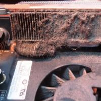 The laptop itself turns off, what to do?
 HP Pavilion DV6: Characteristics and Reviews
 Format representation of a floating point numbers How negative numbers are stored in the computer's memory
 Computer fries and does not turn on what to do?
 Why does not work mouse on a laptop or mouse?
 How to increase or decrease the scale of the page (font) in classmates?