Comparison of NVIDIA chipsets. NVIDIA NForce family chipsets. Processor supply voltage, in
The built-in graphics of the new generation came first on the AMD platform. Why is that? There is no secret here.
First, system logic for the AMD platform is much easier than for the Intel platform. For the reason that the most complex components are already built into the central processor, and the share of the motherboard chipset accounts for only peripheral support. Consequently, to embed a more complex graphics core in the chipset northern bridge crystal for the AMD platform is much easier technically.
Secondly, Intel, the main supplier of chipsets for its platform, has not yet been able to present a decent graphics core, which NVIDIA should be feared. It is not surprising that the leadership of the latter demanded to make every effort to make timely release of new integrated chipsets for the AMD platform. After all, the AMD itself, having got the development department of the ATI chipsets, began to actively develop precisely the direction of integrated decisions. And the chipset with the new graphics core, called AMD 780G, released the first it is.
However, Nvidia pulled up pretty quickly. And, judging by indirect signs, her chipset turned out to be more reliable and brought to mind, although more expensive. Actually, the chipset is not one - their whole line, from the simplest and cheap up to full-featured Tri-SLI support. Of these, the GeForce 8000 chipsets are targeted to the home media centers market, which are designed to install on motherboards with the maximum number of multimedia functions.

So, what can we offer a GeForce 8200 chipset, basic in the mentioned line? It is equipped with a trimmed G86 graphics core, successfully applied in its time in the GeForce 8400 series video cards. The declared support for DirectX 10 and Shaders version 4.0 is unlikely to use the owner of the integrated motherboard, as there are no local memory (in particular, there is no local memory - Only system, available through a common controller) Performance in 3D will be quite low. But on the other hand, the G86 chip is capable of hardware processing the video stream compressed by new codecs, thereby accelerating the playback. At the same time, the new chipset fully supports the HDMI interface for connecting digital TVs, allows you to transmit digital multi-channel sound and video to the same interface.
The new feature of "hybrid" graphics may also seem important, which allows you to add a discrete video card to a joint 3D graphics (GEFORCE BOOST). True, it will work only for the younger model like the same 8400, the purchase of which, between us, does not make any sense. If you equip a new board with a powerful video card class 9800 gt, the hybrid technology can be applied to another - to turn off this video card when operating in 2D, which gives a decrease in the temperature and noise of the computer.
From the point of view of the periphery support, NVIDIA chipsets have long been all in order - gigabit Ethernet, RAID up to level 5, 12 USB ports. The new line is implemented support for PCI Express 2.0. Obviously, the situation remains only with EXTERNAL SATA: on charges with NVIDIA chipsets, the corresponding connector is found if it is served by an additional controller, not a chipset. But the models of external hard drives with EXTERNAL SATA are no longer uncommon.
Gigabyte M78SM-S2h. Design, functionality
Despite the fact that the chipsets of the GeForce 8000 series are practically not inferior to the AMD 780G chipset, and other models of the new generation are very good, Gigabyte preferences exactly the chipsets AMD 700-Oh series. This is due, possibly with a high cost of NVIDIA chips. In particular, on the basis of the GEFORCE 8200 chipset, Gigabyte has (at the time of article preparation) only one model - M78SM-S2H.


And this model is interesting. Let's start with the fact that it is equipped immediately three video outputs - Analog VGA (with D-Sub connector) and digital DVI and HDMI. It should be noted that the digital ports divide one CRTC controller for two, that is, output the same image, while the VGA port works independently of them. This disadvantage can manifest itself, for example, the inability to implement the "Theater" mode when a full-screen video is displayed on the TV, which on the monitor at the same time is played in the window.
On the other hand, there is no support for FireWire (1394), although most video cameras are connected through it. On the ports panel there is a trimmed up to three set of analog "Jacks", but electrical S / PDIF is displayed.

It turns out that the manufacturer recommends connecting both the TV and the sound "on the digit". Audio codec Realtek ALC888 is a regular 8-channel codec with support for basic functions. Network codec is also REALTEK, with support for gigabit networks. The rest of the functionality, including support for hard drives, is provided by NVIDIA chipset.
Read more Consider the design.

The board is made in the MICROATX form factor, but in width it is cut by almost 3 cm. Unfortunately, only two DIMM slots fit, which would not be critical for the entry level board, but the Gigabyte model is not cheaper. A set of other slots is typical for this form factor - one PCI Express, X16 and X1, plus two PCIs. All six SERIAL ATA ports are divorced, like all 12 USB ports (including 8 through internal pin connectors).
The processor power supply module is made using a 4-phase diagram, dynamic phase control is not implemented.

The chains use solid-state capacitors, but only for VRM processor. Both power connector are located at convenient locations.
To cool the chipset, or rather, a single MCP78S chip, from which the GeForce 8200 consists of a large aluminum radiator, painted "under gold".

In order not to interfere with the installation of the expansion card in the PCIE X1 slot, which is only one card, the radiator in the appropriate Spile location.
All connectors are located at convenient locations, with the exception of Front Audio, which is brought closer to the audio model. The peculiarity of the latest Gigabyte models, and the M78SM-S2H in particular, is that all connectors are not only painted in detail, but also provided with signatures directly on the pads (large and readable), as well as frameworks for reliable fixation.

Let's hope that other manufacturers will begin to put such pads.
The panel of ports from the board is non-standard. We have already mentioned three video output and S / PDIF, as about 4 USB ports. There is also an archaic port LPT (hard to assume why it may need in a home computer), but there is no PS / 2 port for a mouse - there are two USB in its place.
BIOS, settings
By tradition, the M78SM-S2H fee is equipped with Award BIOS, which made some branded changes. For example, the most "dangerous" options are available after pressing Ctrl-F1 in the BIOS SETUP main menu.
To enhance performance and overclocking, look at the MB Intelligent Tweaker section, because in the other sections, nothing interesting was detected.

The volume of settings for overclocking is very small and includes:
- the selection of the HT bus reference frequency from which the processor's clock frequency depends (by default 200 MHz);
- the choice of a multiplier (for the Black Edition series processors);
- choosing a multiplier (in the form of frequency) and the width of the HT channel between the processor and the chipset;
- setting the PCI Express bus frequency;
- changing the voltage on the processor and memory modules; The processor displays the rated voltage (so to speak, for reference).
In the memory management subsection, you can specify the desired frequency of its frequency (400, 533, 667, 800 or 1066 MHz), which will not always coincide with the real (due to the features of memory clocking in AMD processors).

A set of timings is hidden from the user, you can only change Cas Latency.
In the PC Health Status section, it is possible to specify the temperature threshold again by the tradition of which the "siren" turns on, and activate the warning about stopping the processor cooler and fan in the case.

Controlling the rotation of the processor cooler is available, but it is not configured; The fan in the case is not controlled.
In general, the M78SM-S2H M78SM-S2H settings set is extremely modest for home appointment and rather characterized for office card.
Equipment
In a box with a Gigabyte M78SM-S2H board, a CD (drivers and utilities for boards on NVIDIA chipsets), a plug for ports panel, two Serial ATA cables, one IDE and one FDD.

The user's manual is very detailed, there is a small instruction in French and Turkish (apparently, these countries are prohibited from selling goods without instruction). No other accessories that can be useful to the user are in the kit.
Testing
We conducted a Gigabyte board testing as part of a computer next configuration:
- athlon 64 x2 5000+ Black Edition processor (2.6 GHz);
- dDR2 GoodRam Pro DDR2-900 2 x 1 GB;
- wD Caviar SE 250 GB hard drive.
For comparison, we give the test results of the competing product - the Micro-Star board on the AMD 780G chipset. This fee is inferior to the M78SM-S2H (no support for RAID and DVI connector), and something exceeds, including in terms of cost.
Performance. In the SYSMARK 2007 test, a number of modern applications are involved, which work out this or that scenario is a sequence of user actions. We launched this package and Windows XP, and in Windows Vista.


And, apparently, the GIGABYTE fee is 5-10% higher. The return result was observed only in Vista, in the scenario of a video editing, which is to blame the SYSMARK 2007 itself rather.
But with the performance of embedded graphics in 3D games for this board (and all analogues) problems.

You can count on playability only in QUAKE 4 or Call games for Duty 2, and even then with minimal settings and resolution below 1024x768. In the built-in graphs of the AMD 780G chipset, the indicators are better, but also far from the desired.
Acceleration. The M78SM-S2H board is capable of working with the support frequency of the HT bus equal to 405 MHz (If the processor allows, of course). The value above this BIOS simply does not allow you to enter. As for the specific results of overclocking the Athlon 64 x2 5000+ test processor, we turned out the result of only 2.75 GHz, or 6% increase. And all because the BIOS does not allow voltage vcore above 1.55 V.
The Gigabyte M78SM-S2H board is interesting primarily by the presence of three outputs at once on the monitor, including HDMI. Its embedded graphics is capable of supporting 3D games (albeit in minimal capacity), as well as hardware decoding HD video on Blu-ray disks. Pluses will also write support for RAID and the presence of six SERIAL ATA connectors. At the same time, this fee is not suitable for overclocking (at least with an activated embedded graph) and does not have any additional functions that are put on a good model for home PC.
Pros:
- three video outputs;
- practical layout, reduced width;
- 6 ports Serial ATA and 12 USB;
- solid-state capacitors in the VRM processor chains.
Minuses:
- only two DIMM slots;
- no firewire;
- the analog connection of acoustics 7.1 is not supported;
- poor BIOS settings.
We thank the company "Jethsservice" for the Gigabyte motherboard provided
| Author's rating: |
|
NVIDIA is well known to PC users as a recognized leader of the game video card market. Thanks to its 3D GeForce accelerators, the company managed to take a practically monopoly position, since it is competing only by one graphic company, ATI Technologies. Without stopping at what happened, Nvidia has attempted to invade another market, the chipset market for motherboards.
However, it is impossible to name this attempt. In my opinion, the situation was repeated with the launch of the NVIDIA graphic business. As you know, the company debuted on the market with the NV1 chip - an integrated controller that combines and video, and the sound part. However, as a result, I had to abandon the sound and release the NV2 (it is riva128) - a classic graphic 3D accelerator.
Of course, today everything is not the way it was at the beginning. NVIDIA is not new to the development of high-tech products. However, the chipsets for motherboards have its own specificity: this is not just a subsystem, as in the case of a graphical controller, this is the most important node of the system, acting as a binder between all other components. Almost all parameters of the system are largely dependent on the chipset - performance, compatibility, extensibility, functionality, stability, etc. From the first time to release the product, which is not inferior in all parameters analogues of firms that did not eat on the development of chipsets, it seems simply unreal.
However, it is necessary to pay tribute to the courage of NVIDIA. The company did not simply proposed his analogue, it used the most advanced and promising technologies, making an application for leadership both in the productive PC segment and in the basic segments (MainStream) and budget (Value) systems. Unfortunately, everything goes to the fact that the attempt as a whole failed. However, this is a little later, and now - a brief overview of the chipsets of the NForce series with a comparison of what Nvidia wanted, and what happened.
Chipsets NForce: 420D, 415D, 220D, 220
The NVIDIA chipset family includes current four basic modifications: NForce 420D, 415D, 220D and 220 (descending value). Also, two more chipset - NForce 620d and 615d will be added in the near future, which are nothing more than the final modifications 420d and 415d, respectively (at least such information are available at the time of writing the article).
The structure of the chipset is a classic two-phase: the conjugation of the processor, memory and the AGP video card is engaged in the northern bridge, and the southern bridge is responsible for working with peripheral devices. Nordic nForce bridges There are three: IGP-128, IGP-64 and SPP.
"IGP" is "Integrated Graphics Processor" (integrated graphics processor), the north bridge with a built-in graphic core, which NVIDIA calls the processor. Ideologically, it is incorrect, since it does not do the data processing, but only commutes data streams and commands. Here it is part, the graphic core is indeed a processor. Options of the chip with indexes -128 and -64 are distinguished by the total width of the memory bus (about that below). The IGP-128 chip is the basis of NForce 420D, and IGP-64 - NForce 220D and 220.
SPP is decrypted as "System Platform Processor". In fact, it's all the same IGP-128, but with a disconnected graphics core. Nvidia had to abandon the built-in graphics, quite slowly according to the current standards, since it does not satisfy modern requirements. The market of productive computers did not accept the NForce 420D, however, in the case of NForce 415D (this chipset uses the North Bridge SPP) The situation may change in a radically. Something similar at one time happened to Intel and the I815 chipset. For example, it is not clear to me why Nvidia has stepped on the same rake.
As a southern bridge NVIDIA offers a MCP-D chip or its simplified MCP version. "MCP" is decrypted as "Media and Communication Processor". It includes a NVIDIA "AUDIO PROCESSING UNIT), USB and ATA, PCI and LPC interface controllers, a MAC-level network controller, a SMBUS controller, other controllers and something unusual - a clock generator. Communication with the Northern Bridge is carried out via the Hypertransport bus - in fact, this is the first mass product that has support for this latest AMD development.
Let's consider the features of the architecture and operation of chips.
North Bridges IGP and SPP: Twinbank, Dasp, NV11
The NForce 420D chipset north bridge is a chip that provides processor, memory, AGP video cards and MCP bridge. It consists of the following blocks:
- tire interface (support for EV6 tires with an effective frequency of 200 and 266 MHz, used by AMD K7 processors);
- aGP host controller (4x, FastWrites, SBA modes, frequency 66 MHz);
- hypertransport bus controller (for communication with MCP, bandwidth is 800 MB / s);
- two independent memory controllers, support for SDRAM and DDR SDRAM, frequency - up to 133 MHz, volume - up to 1.5 GB;
- built-in GPU graphics core (NV11 GeForce2 MX);
- intellectual arbiter switch.

Nforce chipset supports AMD Athlon and Duron processors. However, NVIDIA does not have any technical problems with the implementation of support for other processors, in particular, Intel Pentium-4. For a number of reasons - marketing, legal, etc. - At the moment there is only a version of the chipset for the AMD platform.
The built-in graphical core is completely equivalent to the NV11 chip (GeForce2 MX). Differences only in clock frequencies and memory interface. The built-in kernel uses system controllers that provide memory access to other components of the system (primarily the processor). The graphic core can be disabled if an external video card is installed in the AGP slot. For most users who use games or graphic applications, opportunities and speed GeForce2 MX will not be enough.
To implement the output to the TV and digital monitor, the chipset supports special extension boards installed in the AGP slot. However, they are not much common, so it is hardly possible to take this opportunity.
The SPP chip differs from IGP only disabled built-in video.
Twinbank. - The key feature of the architecture of Nforce, due to which, actually, the performance of the chipset was to be quite high. Its essence is that the chipset does not have one, but two full-fledged independent 64-bit memory controllers to which all blocks of the chipset can turn. Each of the controllers works with its set of banks (first - with dimm0, the second - with DIMM1 and DIMM2). Data is located in all banks with alternation. When consistently accessing memory, the device will receive data from both banks alternately in the conveyor mode, which will reduce delays associated with the opening / closing of pages, delays in regeneration, etc. If several devices immediately appear to the memory, they do not have to stand waiting until the controller is completed with another device. Thus, it is guaranteed an increase in the speed of working with memory and an increase in its peak bandwidth to 4.2 GB / s.
The use of such an architecture should not lead to a significant increase in the performance of the entire system for the simple reason that the capacity of the EV6 processor bus is only 2.1 GB / s - an additional 2.1 GB / with it almost nothing will be given. The TwinBank architecture is optimized primarily for the needs of the built-in graphics core. Thanks to it, the integrated GeForce2 MX will be less susceptible to the challenges of the memory bus separation with other components of the system, primarily with the processor. If a separate video card will be used, the speed increase will be noticeable, since the collapse of the AGP channel textures is usually not so intense to load the system memory.
NVIDIA argues that if you only install one DIMM module, only one memory controller will be used. Therefore, it is desirable to put two modules - one in the first one, the other in the second slot. Since controllers are independent, you can put different modules and configure them separately. According to some information, if the memory modules are not recognized as officially supported (see the list of compatible modules on the NVIDIA website), the "Super Stability Mode" mode will be activated, in which the memory timings are reduced. Thus, NVIDIA struggles with the problem of low stability of its chipset identified immediately after the first motherboards at its base.
The IGP-64 chip does not allow you to use TwinBank (the second memory controller is disabled), so its embedded video may be theoretically reach only the level of GeForce2 MX200. However, until recently, the NForce 220D based on the IGP-64 chip is not claimed due to too high prices, disproportionate with its functionality and productivity.
Another key feature of the IGP chip (more precisely, its arbiter) - an analyzer of memory appeals Dasp. Dynamic Adaptive Speculative Pre-Processor). It monitors read requests, analyzes their character and builds patterns with which you can predict subsequent requests. After the template is defined, the DASP block begins to generate requests yourself, predicting them and caching the data obtained. Thus, the memory bandwidth is used more efficiently, and part of the data, which is properly predicted and received from the memory in advance enters the processor without accessing memory. Existing chipsets are only able to set requests to queue, but not to predict them. Thus, the DASP technology should increase the efficiency of TwinBank and provide data output from memory with smaller delays.
South Bridge MCP: APU
The South Bridge NVIDIA MCP is connected to IGP / SPP using the new Universal Hypertransport bus, the main advantage of which in this case is high throughput (800 MB / s). Only the SIS chipsets have a faster-in-free bus - Mutiol (1 GB / s), and that outside the chips is twice as slower.
MCP - a typical modern southern bridge, having in its composition PCI controllers (up to five slots), LPC (connecting flash microcircuits with ROM and I / O chip), USB (up to six ports), ATA / ATAPI (UltraAta / 100 mode) , MAC-level network controller and two AC interfaces for sound and modem codecs. But there is a bridge and a unique feature - a built-in sound controller APU Audio Processing Unit). It is based on a multiple DSP and is capable of hardware processing up to 256 2D-sound streams, up to 64 3D-sound streams, apply various special effects, including HRTF filters (for imitation of surround sound). APU supports DirectSound3D and new features DirectX8, as well as APIs and algorithms of Sensaura. In addition, and this is implemented for the first time, the NVIDIA sound controller has a built-in audio encoding unit into Dolby Digital digital format (AC-3), which makes it possible to effectively use the user's digital acoustics or the "home theater" system. However, this unit works only at the MCP-D chip (NForce420D), and the MCP is disabled.
What's the problem?
Well, you will tell you, the wonderful chipset is two memory controllers, the Hypertransport bus, more than an advanced built-in sound, and the graphics core - the best today. Why then we are not littered with fees on NForce chipsets?
There are several reasons for this. First, the chipset is very expensive. Nvidia asked for him unrealistic money, so manufacturers of motherboards focused on a poor user immediately abandoned Nforce - their potential customers simply will not be able to buy expensive fees. Today, NVIDIA collaborates only favorites companies with a positive reputation that release the upper price ranges - ASUS, ABIT, MSI, LEADTEK, etc.
Secondly, the chipset was not too successful. Here is just a short list of his problems:
- unable to prepare BIOS, which is why there are problems with compatibility, speed and stability;
- the built-in clock generator does not have extensive adjustment capabilities, which limits the suitability of the acceleration board;
- not provided sufficient funds to configure the chipset;
- driver-level support leaves much to be desired: WinNT, Linux and some other OS are practically not supported, Win98 / ME - only partially (for example, hardware sound works with grief in half).
Thirdly, the chipset did not fit into that niche, which was aimed at. The built-in playing video turned out to be inappropriate at a high price - much more important it is for the budget machine, but not for an expensive game or workstation. In my opinion, instead of NForce420D, it was necessary to immediately release a pair of NForce 415D + NForce 220D.
However, the NForce 420D database boards after almost the year the finished finally came on sale in sufficient quantities. One of the following articles will be devoted to the review of one of them.
Equipment.
In a colorful box, impressive sizes, except the motherboard had:
1. SLI bridges for 3-way and normal 2-way SLI mode.
2. HDMI-TO-DVI adapter.
3. Additional fan for motherboard.
4. Adapter for connecting fans.
5. Pinches Ultradma 133/100/66, SATA CABLES.
6. SATA power cables.
7. Extra charge with 2 USB 2.0 and IEEE 1394A
8. Manual for operation.
9. Disk with drivers and programs from ASUS, 3DMark06 and that I was especially surprised, with Kaspersky Anti-Virus!
10. Disk with the game Company of Heroes - Licensed full version. Technical specifications.
The following features are stated for the new motherboard from ASUS:
1. AMD® Socket AM2 + for AMD Phenom ™ FX / PHENOM / ATHLON ™ / SEMPRON ™ processors
2. AMD Socket AM2 for AMD Athlon 64 X2 / Athlon 64 FXLON 64 / SEMPRON
3. AMD COOL "N" QUIET ™ TECHNOLOGY
4. CHIPSET NVIDIA® NFORCE 780A SLI
5. System Bus Up to 5200 MT / S; Hypertransport ™ 3.0 Interface for AM2 + CPU. 2000/1600 MT / S for AM2 CPU. As you can see, a new tire is used here, this is the first difference from the parent cards of the previous series.
6. Memory 4 x Dimm, Max. 8GB, DDR2 1066/800 / 667, ECC and non-ECC, Un-Buffered Memory. There is a second difference. True, this is not the merit of a new chipset, but the merit of new AMD processors. Due to the fact that new processors, the memory controller supports memory with a frequency of 1066MHz and the motherboard when installing new processors will support it.
7. DUAL CHANNEL MEMORY ARCHITECTURE
8. VGA INTEGRATED GRAPHICS. And here we see new NVIDIA tactics, when it was this: top motherboard with integrated video? And this is done everything to support new technologies Hybrid SLI and Hybrid Power.
9. 512MB MAXIMUM SHARED MEMORY OF MB Supports HDMI ™ Technology with HDCP COMPLIANT WITH MAX. Resolution 1920 x 1200
10. Supports D-Sub With Max. Resolution 1920? 1440 @ 75 Hz Multi VGA Output Support: DVI & D-SUB
11. Hybrid SLI Support
12. Expansion Slots 3 x PCIE2.0 X16 Support NVIDIA SLI Tech @ Dual X16 OR [Email Protected], x8, x8. This is another difference of the 3-slot PCI-EXP.
13. 2 x PCIE X1, PCIEX1_1 (Black) IS Compatible with Audio Slot 2 x PCI 2.2
14. Storage 6 X SATA 3GB / S Ports WITH RAID 0, 1, 0 + 1, 5 AND JBOD Support
15.1 X ULTRA DMA 133/100 / 66/33
16. Lan Dual Gigabit Lan Controllers, Both Featuring AI Net2
16A. High Definition Audio Supremefx II Audio Card
- ADI 1988B 8-Channel High Definition Audio Codec
- Noise Filter.
-Coaxial, Optical S / PDIF Out At Back I / O
17. IEEE 1394 2 x 1394A Ports (1 Port at Back I / O, 1 Port Onboard)
18. USB MAX. 12 USB2.0 / 1.1 Ports (6 ports on the motherboard, 6 ports on the body)
19. ASUS ROG OVERCLOCKING FEATURES EXTREME TWEAKER
20. New 8 + 2 phase power system.
21. Utilities for overclocking:
- CPU LEVEL UP
- AI OverClocking (Intelligent CPU Frequency Tuner)
- ASUS AI Booster Utility
- O.C PROFILE
22. Overclocking protection system:
- COP EX (COMPONENT OVERHEAT PROTECTION EX)
- Voltiminder LED
- ASUS C.P.R. (CPU Parameter Recall)
23. ASUS ROG Special Features LCD Poster
24. ROG BIOS WALLPAPER
25. Onboard Switches: Power / Reset / Clr CMOS (AT REAR)
26. Q-Connector
27. ASUS EZ FLASH2
28. Asus CrashFree BIOS2
29. Stack Cool 2
30. ASUS Q-SHIELD
31. Asus mylogo3
32. Only tidicultural capacitors are used.
33. Input ports on the rear panel:
1 x HDMI
1 x D-Sub
1 x PS / 2 KEYBOARD PORT (PURPLE)
1 x Optical + 1 x Coaxial S / PDIF OUTPUT
2 x LAN (RJ45) Port
6 X USB 2.0 / 1.1 Ports
1 x IEEE1394A port
1 x CLR CMOS SWITCH
34. Internal ports:
3 X USB 2.0 Connectors Supports Additional 6 USB 2.0 Ports
1 x FLOPPY DISK DRIVE CONNECTOR
1 x IDE Connector for Two Devices
6 X SATA Connectors
8 x Fan Connectors: 1 x CPU / 1 x PWR / 3 X Chassis / 3 x Optional
3 x Thermal Sensor Connectors
1 x IEEE1394A Connector
1 x S / PDIF Output Connector
1 x chassis Intrusion Connector
24-PIN ATX POWER CONNECTOR
8-PIN ATX 12V Power Connector
1 x EN / DIS-Able CLR CMOS
1 x LCD Poster
1 x ROG LIGHT CONNECTOR
System Panel Connector
35. BIOS 8MB AWARD BIOS, PNP, DMI2.0, WFM2.0, SM BIOS 2.4, ACPI2.0A Multi-Language BIOS
36. ManageAbility Wol by PME, China by PME, Chasis Intrusion, PXE
37. Form Factor ATX FORM FACTOR, 12 "X 9.6" (30.5cm x 24.4cm)
Overclocking
On the new motherboard, the Phenom 9850 processor, it was easily able to conquer its cherished 2, 94 GHz on a nominal voltage of 1.25 V ..
With increasing voltage, the cooler did not cope with its function, so it was decided to abandon this manipulation. Test configuration and test results.
Test configuration:
1. ASUS CROSSHAIR II FORMULA
2. AMD Phenom 9850 Box
3. Gainward 8800 GTS 512MB Blitz
4. 2x1gbsamsung PC6400 DDR800
5. 2xHD WD 250AAJS in RAID 0 array.
6. Case Colors-IT
7. BP FSP 450W
8. ASUS 222U Monitor
Testing was conducted in the following tests:
2. PC MARK 2005.
3. 3DMark 06.
1. Crysis (all per maximum resolution 1280x1024)

As you can see, the new Tire Hypertransport 3.0 gives its results. The new chipset shows decent results.

In the synthetic test, the new chipset also demonstrates the outpacing results.

In this test, we also see the advantage of a new chipset. Immediately should make a reservation, - the advantage goes at the expense of the processor test.
4. Test hard disk from the EVEREST ULTimate package.

Linear reading speed with RAID 0 array is also higher than that of the previous chipset.

Access time on hard drives, also faster on a new chipset. Conclusions:
1. The new chipset shows excellent performance results. In all tests, he turns out to be the fastest of the predecessor.
2. Especially pleased increase the speed of working with hard drives. I have recently paying more attention to this, as I think that in the modern computer, the fastest place is hard drives.
3. It is a pity, but the cooling system of the processor did not allow for all overclocking qualities of the motherboard and processor. But I am sure, the acceleration characteristics of the processor would not be as stunning as the triumph of a new chipset.
4. All the above overshadow, only new AMD processors are overshadowed. Yes, if you do not plan overclocking - you can buy a new motherboard with an AMD processor. But on the other hand, it is worth paying $ 600 for a bunch of motherboard and processor. Yes, of course, you can take a processor cheaper. But it is not logical to buy a motherboard for $ 330, and the Phenom X3 processor for $ 170 or Athlon X2 for $ 100.
5. Hence the output - this motherboard is great for AMD fans and no more.
6. We, prudent users, Let's wait for motherboards at the NForce 750a SLI chipsets, the benefit of motherboards on new NForce 750i SLI chipsets are already available on sale.
The article is prepared FireAid especially for Mega Obzor.
See this article:
Video cards based on NVIDIA GeForce RTX 2070, which is devoted to this material are low models from the new generation graphic adapters already submitted on these data with the NVIDIA Turing architecture.
If you do not take into account the very specific NVIDIA Titan RTX worth $ 2500, then user video cards with NVIDIA Turing architecture are represented by the NVIDIA GeForce RTX 2080 Ti, RTX 2080 and RTX 2070 family. These are high-class video cards, and after a while it is planned to appear and simpler type devices RTX 2060.
We look at the characteristics
Graphic processors for new video cards Turing are performed on a more "thin" 12-nanometer process. But, according to rumors, this technical process is not something fundamentally new, but represents only a slightly refined version of the 16-nanometer technical process, which is used in the predecessors.
For convenience of comparison, the characteristics of the new GeForce RTX 2080 Ti, RTX 2080 and RTX 2070 and the predecessors of GeForce GTX 1080 Ti, GTX 1080 and GTX 1070, we reduced them into one table.

From generation to generation NVIDIA video cards, you can observe the cost of video cards. But if earlier it was rather smooth, then in this case the NVIDIA Turing adapters significantly exceeded the predecessors for the price.
What do we pay?
In part, this increase can be explained by the increased complexity of new GPUs. Please note that they have a highly increased amount of transistors and a significantly higher crystal area. Accordingly, it can be assumed that the cost of such crystals is higher.
There are some deviations by the values \u200b\u200bof the GPU frequency. Memory is now new. Instead of GDDR5x and GDDR5, the RTX video card received GDDR6.
But it is noteworthy that the amount of memory in the new generation of video cards remained at the same level as the predecessors.
It is very important that completely new RT kernels and tensor kernel appeared. This is exactly what such an increase in the number of transistors and the GPU crystal area is due.
Rays tracing
Generation of RTX 2080 TI, RTX 2080 video cards, RTX 2070 based on the Turing architecture, NVIDIA itself calls a revolutionary and binds it with hardware support for tracing rays in real time.
For this, the RT nucleus mentioned above is introduced. Nvidia considers it so important that the usual GTX console in new video cards was even replaced by RTX, where RT - Ray Tracing (rays tracing).
This technology at the presentation of video cards of the new generation was given almost the main attention.
If simplified, then with Ray Tracing, new effects of reflections on objects (including mutual), light reflections and rays through objects are connected. At the same time, rays can have realistic refraction, imposition, etc. Ray Tracing also allows you to use more realistic softened shadows and form believable lighting.
This is really a very important innovation for the industry, but, no matter how paradoxically, it is with the Ray Tracing technology and connect a rather cold reception of new video card users.
New RT-cores made crystal larger and expensive, and what users get in return?
At the time of the release of RTX video cards there was not a single game that would have supported Ray Tracing. Now the situation changes, but very slowly.
For example, try ray tracing in general in any game it became possible quite recently with the release of Battlefield V.
As it turned out, the picture in Battlefield V with effects is not changing and dramatically. There are improvements, but you will not say at all that you get a fundamentally new level of perception.
But Ray Tracing Computing Resources "Harvested" is essential. When the ray trace is activated, the performance may fall more than twice.
As a result, even with the most expensive top NVIDIA GeForce RTX 2080 Ti, the FPS level with Full HD-resolution, maximum quality settings using Ray Tracing will not always be able to satisfy demanding gamer.
And then what to talk about simpler RTX 2080, RTX 2070 and higher permissions?
Turns out that at the moment There are practically no games with ray tracing games, visually the difference in the image with RT effects is not so cardinal, and the activation of trace leads to a large drop in the FPS level.
For Ray Tracing users in real time, only is only potentially promising technology. Let's see how the situation will develop.
DLSS smoothing, tensor nuclei and artificial intelligence
In addition to a completely new RT nuclei in RTX video cards, tensor kernels appeared, intended for calculating AI and neural network. They work in a bundle with RT nuclei, but tensor kernels can be used for other functions.
On the basis of their work, a new smoothing method is implemented - DLSS (Deep Learning Super Sample). A reduced resolution of rendering is used, but at the expense of the AI \u200b\u200band the tensor cores of the video card converts the image to a better, "impairing" new details.
Depending on the implementation of the implementation, due to this, it is possible to achieve an increase in productivity, improve image quality or both at the same time.
Again, as in the case of ray tracing, support from games is needed for DLSS. It is indicated that several dozens of game-preparing games will support DLSS smoothing.
One of the few tests, where you can check DLSS now, Benchmark Final Fantasy XV Benchmark has become. If the GEFORCE RTX video card is installed in the system, the appropriate item appears in the settings that allows you to activate the DLSS.

According to our tests, the activation of DLSS led to a significant increase in productivity.

Image quality using DLSS and with the usual TAA smoothing in this application is comparable. You can independently compare frames with DLSS and with TAA.
 Dlss.
Dlss.  TAA.
TAA.
What are other news?
The technology of automatic increase in the frequency of GPU continues to be improved. The Fourth Generation of GPU Boost is used in NVIDIA RTX video cards.
Added the ability to manually adjust the acceleration algorithm. But much more interesting is that the function of automatic overclocking appeared for the first time.
If earlier to determine the limit frequency of the GPU was required to experiment, run various games, applications, now the process can be greatly simplified.
NVIDIA Scanner is available in MSI Afterburner applications. By pressing only one button, after 15 minutes of automatic tests, you will receive a modified GPU frequency / voltage curve, respectively, with higher frequency values.
In our tests for all RTX 2070 video cards, we checked such automatic acceleration. Of course, to obtain even higher overclocking results, you still have to carry out more complex dispersal "manually".
RTX video cards can be connected at once two monitors with a resolution of 8K. Maximum frame frequency will be 60 Hz in both image output devices.
DisplayPort ports now correspond to the versionPort 14a versions, and HDMI - HDMI 2.0B. Also also pay attention to the USB Type-C connector directly on the video card. It is intended for new VR helmets.

However, this port can be used for any device with USB Type-C support.
It is quite expected to work with various video codes. For example, support for data compression in H.265 format (HEVC) is added in permission mode, as well as encoding quality. Considering that today video cards are actively used when video editing, it is very relevant.
The ability to combine multiple video cards in one system is now available only in high-class video cards. NVIDIA GeForce RTX 2070 such a function is deprived.
Participants dough
In one test, we managed to collect four video cards based on NVIDIA GeForce RTX 2070 from different manufacturers.
This ASUS ROG STRIX GEFORCE RTX 2070 OC EDITION, GIGABYTE AORUS GEFORCE RTX 2070 XTreme 8G, Inno3D GeForce RTX 2070 Gaming OC X2 and MSI GeForce RTX 2070 Gaming Z 8G.


All of them have significant differences from the reference RTX 2070, received elevated frequencies and use branded cooling systems.
Comparative table characteristics
| Code identifier model | ROG-STRIX-RTX2070-O8G-Gaming | GV-N2070AORUS X-8GC | N20702-08D6X-2511683. | - |
| Provider | Representing asus | Representing Gigabyte | Represents Inno3D | Representing MSI |
| Price, $ | 796 | 742 | 675 | 725 |
| Measurement results | ||||
| Performance | 87,49 | 87,73 | 86,21 | 87,93 |
| 100 | 96,91 | 98,54 | 98,79 | |
| Manufacturing / price | 86,7 | 93,26 | 100 | 95,66 |
| Specifications | ||||
| Chipset | NVIDIA GeForce RTX 2070 | NVIDIA GeForce RTX 2070 | NVIDIA GeForce RTX 2070 | NVIDIA GeForce RTX 2070 |
| Chipset technical process, nm | 12 | 12 | 12 | 12 |
| Type and size of memory, GB | GDDR6, 8. | GDDR6, 8. | GDDR6, 8. | GDDR6, 8. |
| Design of cooling system | branded | branded | branded | branded |
| Number of fans cooling system | 3 | 3 | 2 | 2 |
| Number of slotted | 3 | 3 | 2 | 3 |
| Subjective assessment of cooling noise | Excellent | Excellent | Okay | Excellent |
| Nominal frequency GPU. | 1410 | 1410 | 1410 | 1410 |
| BOOST-FREQUENCY GPU | 1815 | 1815 | 1755 | 1830 |
| Resulting frequency of memory, MHz | 14000 | 14142 | 14000 | 14000 |
| Memory bus, bit | 256 | 256 | 256 | 256 |
| Requires additional nutrition? | yes | yes | yes | yes |
| Type of Extras connector. Nutrition | 6pin + 8pin | 6pin + 8pin | 6pin + 8pin | 6pin + 8pin |
| Number of HDMI / DisplayPort / USB Type-C outs | 2/2/1 | 3/3/1 | 1/3/1 | 2/2/1 |
ASUS ROG STRIX GEFORCE RTX 2070 OC EDITION (ROG-STRIX-RTX2070-O8G-GAMING)

Presented in Test ASUSROG.Strix.GeForce.RTX 2070.OC.eDITION is currently the most powerful in terms of frequency.GPU and advanced among all video cardsAsus on the baseRTX 2070..
It has a traditional for ASUS ROG STRIX design, which has practically not changed since the past generation.

The device was quite large and the system will take three expansion slots.
It uses a modified board with a phase configuration of 10 + 2 and a branded cooling system with three fans.
As declared, the fans have a special design, and the insides are protected from dust. By the way, the direction of rotation of all fans is the same.


The massive radiator C is permeated with six thermal tubes. The outlet of the heat receiver has a special processing that ASUS calls MaxContact technology.
When examining ASUS ROG STRIX GEFORCE RTX 2070 OC Edition (ROG-STRIX-RTX2070-O8G-Gaming), curious parts are found on all sides.
Two microcircuits are installed on the board at once.Bios. With a bit modified board work modes. One of them (Performance) provides increased cooling efficiency, which is achieved by higher fan operation speeds, and the second (quiet) is designed for more quiet operation. The BIOS selection is made by a special switch.

By the way, the full stop of the fans at low load becomes only when using the BIOS option with Quiet mode.
At the end, a special button is displayed for quickly disconnecting / turning on the backlight. This is a good solution when you need to pay off the glow without the use of corporate software.
Also, the board provides a platform for manual measurement of the RAM, GPU, PLL voltage and a set of contacts for connecting LED tapes and body fans. The speed of rotation of these fans can be associated with the GPU temperature. This is a cool feature.

On one of the sides of ASUS ROG STRIX GeForce RTX 2070 OC Edition, you can notice the contacts to connect LED tape and body fans


The frequency of memory in this model corresponds to the reference, but the GPU boost frequency is increased very significantly - from 1620 to 1815 MHz.
As a result, ASUS ROG STRIX GEFORCE RTX 2070 OC EDITION is among the leaders of the performance test. Clean the Gigabyte Aorus GeForce RTX 2070 Xtreme 8G and MSI GeForce RTX 2070 Gaming Z 8G in speed failed, as all three models, including ASUS, have similar operating frequencies. Very strong video cards participate in the test.

Monitoring ASUS ROG STRIX GEFORCE RTX 2070 OC EDITION in the MSI Afterburner
When working under load in our conditions, the temperatureGPU made up only 57 °C.. For all performance tests and measurement tests, a BIOS was used with Performance mode.
Given the fairly high energy consumption of the video card, it is just a great result. By the way, this is the lowest temperature value among all tested video cards based on RTX 2070 in this test.
The speed of rotation of the fans amounted to about 1600 rpm. When the video card does not create noise discomfort.
When using automatic acceleration with initial settings, the maximum frequency of the GPU almost reached 2100 MHz.

ASUS ROG STRIX GEFORCE RTX 2070 OC EDITION allows you to increase the power limit up to 125%. This is the highest value in the test.

The backlight system consists of several elements with RGB-backlight on the front panel, luminous by the ASUS ROG logo on the side and another large logo derived from the back plate.


Working backlight, of course, can be controlled. A number of effects are available, as well as the ability to change the color, depending on the GPU temperature.

Feature: The color of the glow can change, but at the same time all illumination elements have the same color.
It is quite nice, but today there are also more advanced solutions, including among the test participants. The backlight of the video card Gigabyte Aorus and MSI turned out to be even coolest.

Corporate on ASUS in terms of opportunities is about to combine MSI Afterburner and GPU-Z
ASUS ROG STRIX GEFORCE RTX 2070 OC Edition is a very powerful video card based on RTX 2070 with an easy-to-other cooling system.
It is among the leaders in performance, has a number of curious additional functions in the form of two BIOS chips, contacts for the fans of the housing and the LED tape.
But with all its advantages, ASUS ROG STRIX GEFORCE RTX 2070 OC Edition has the highest cost among other dietary participants based on RTX 2070.
Asus ROG STRIX GEFORCE RTX 2070 OC EDITION (ROG-STRIX-RTX2070-O8G-Gaming):
Excellent cooling system
Energy consumption limit higher than other participants
Double BIOS.
Contacts for connecting RGB LED tapes and hull fans
- the highest value
- Large dimensions
- relatively modest equipment

If ASUS ROG STRIX video cards in the new generation look almost as well as in the previous one, then MSI his series Gaming modified significantly.
The recognizable design with the predominance of red and inserts, reminiscent of the dragon claws, decided not to use anymore.

The model is not so long, but wide and in the system will take the place of three expansion slots.

MSI GeForce RTX 2070 Gaming.Z 8.G. (Attention to the prefix z in the title) is highlighted by higher frequencies compared to MSI GeForce RTX 2070 twins Gaming.X 8.G. and MSI GeForce RTX 2070 Gaming 8.G.and it is the fastest RTX 2070 for MSI at the moment.


The fee is typical for the Gaming series recycled. Displays the configuration of power phases 8 + 2. Co consists of two fans and a powerful radiator with six thermal tubes.
If you look at, then in each fan alternate the blades of two types. Technology is called Torx Fan 3.0. In combination with the new design of the radiator scattering plates, this, according to the manufacturer, will contribute to better efficiency.

The cooling system really turned out to be very effective.

Fixed temperature under load - 66 ° C. But surprised another. This temperature is kept at the speed of rotation of the fan of only 1100 rpm.
As a result, the video card works very quiet. According to the cooling efficiency, MSI surpassed other participants except the ASUS ROG STRIX GeForce RTX 2070 OC Edition. But with asus it is difficult to compare. On the one hand, a competitor has a lower temperature, and on the other, it is achieved with noticeably higher fan speeds.

The BOOST frequency of the GPU video card MSI GeForce RTX 2070 Gaming Z 8G is 1830 MHz. This is the highest value among all dough participants. But superiority over ASUS ROG STRIX GEFORCE RTX 2070 OC Edition and Gigabyte Aorus GeForce RTX 2070 Xtreme 8G is completely meager. These video cards, this value is 1815 MHz.
Memory frequency, while standard. It is logical that RTX 2070 Gaming Z 8G was among the leaders in performance. With automatic acceleration, the maximum frequency reaches 2100 MHz.

Curves of the frequency and voltage of the graphics processor MSI GeForce RTX 2070 Gaming Z 8G characteristic (GPU-Z application data) with standard settings (top) and after automatic acceleration
An affordable energy consumption limit is 111%.
Very pleased with a new backlight system of this video card. Luminous areas around the perimeter surrounded fans. The logo on the side is highlighted.

The thing is how dynamic effects are implemented here. In some modes, this is a kind, color show. Although there is no luminous element on the back plate. This backlight MSI liked more than the solution at ASUS.


Included with the video card comes with an additional plank for a more reliable fastener of the video card in the housing. The video card is really weighty, but, in our opinion, there is no big necessity in such a bar. It is likely that it does not hurt, when transporting the case.

The bar is screwed into the computer housing below the video card after which the device relies on this bar through soft prolutions
MSI GeForce RTX 2070 Gaming Z 8G is distinguished by high factory overclocking, and an excellent cooling system efficiently, and an interesting new backlight. A good model turned out.
Evaluation MSI GeForce RTX 2070 Gaming Z 8G:
Excellent cooling system
Turning off the fans at low load
Significantly increased GPU frequencies
Advanced RGB-backlight system
Additional fastening bar included
- Large dimensions
Gigabyte Aorus GeForce RTX 2070 Xtreme 8G (GV-N2070aORUS X-8GC)

Even compared to other major video cards in the test Gigabyte Aorus GeForce RTX 2070 Xtreme 8G is still more massive.

Gigabyte Aorus GeForce RTX 2070 Xtreme 8G Left
But the main contribution to the thickness of the device does not bring the CO radiator, but a rather curious placement of fans.


They are located a bit of brass. Thereby, with moderate length, it was possible to place three 100mm fans at once..
GigabyteAorus.GeForce.RTX 2070.Xtreme 8.G is the fastestRTX 2070 at Gigabyte.

Boost The frequency is 1815 MHz, which, however, is comparable to the tested ASUS ROG STRIX GeForce RTX 2070 OC Edition and MSI GeForce RTX 2070 Gaming Z 8G.
It is curious that the factory overclocking received memory. In all other RTX 2070 video cards, this test frequency test is reference.
But memory gain in the case of the AORUS GEFORCE RTX 2070 Xtreme 8G is purely nominal and little affects the final performance. The frequency was raised with a standard 14,000 to 14 140.
The performance of the Gigabyte Aorus GeForce RTX 2070 Xtreme 8G was at the level of MSI and ASUS video cards.
Using automatic acceleration, the maximum value of the GPU frequency was about 2100. What roughly repeats the results of MSI and ASUS.

Curves of the frequency and voltage of the graphics processor Gigabyte Aorus GeForce RTX 2070 Xtreme 8G with standard settings (top) and after automatic acceleration
Available to change the maximum energy limit - 109%.
Power supply system configuration - 10 + 2.
Unlike other participants, in the design of the cooling system instead of a polished plate or evaporative chamber, the option is used when the heat pipes themselves concern GPU.
Total thermal tubes are five.
The manufacturer adds some attention that the central fan has a different direction of rotation compared to extreme. It is indicated that it avoids turbulence and increases the effectiveness of CO.
Care the model and stop the fans at low load. On the sidebar, traditionally for Gigabyte, even withdrawn the inscription "Fan Stop", which lights up when the fans are idle.

How did such a case show yourself?
The fixed values \u200b\u200bof temperature and revolutions under load were 67 ° C at 1700 rpm. It is very good, but it turns out that efficiency with the ASUS ROG STRIX GEFORCE RTX 2070 OC EDITION and MSI GEFORCE RTX 2070 Gaming Z 8G is slightly higher.

The backlight system in Gigabyte Aorus GeForce RTX 2070 Xtreme 8G is very unusual.
On the edge of one of the blades of each fan placedRGB diode. This diode can change the color depending on which sector of the circle it is when the fan is rotated. The resulting effects are impressive.


The video card is really capable of attracting a lot of attention.
Additionally, the logos placed on the front, reverse sides and on the side of the video card are highlighted.
Due to the fact that the backlight of the AORUS GeForce RTX 2070 Xtreme 8G is connected with the rotation of the fans, and not very pleasant features are revealed. First, the effects with rings work only with running fans. Secondly, noticeably a little flicker. The second drawback, however, is not expressed so significant. If the video card is not constantly in your field of view, there will be no inconvenience.


The video card Gigabyte Aorus GeForce RTX 2070 xtreme 8g turned out to be the largest number of video outputs in the country's own video cards based on RTX 2070 in this review
The set showed a leg for reliable fixation of the video card in the case. Yes, a weight video card, but the urgent need for such additional support, in our opinion, is not.


By the way, the level of materials and processing in this leg is simply amazing.
Does this kind of accessories become trend for high-class video cards?

Summarizing, we can say that the Gigabyte Aorus GeForce RTX 2070 Xtreme 8G is highlighted not only by significant factory overclocking, but also a rather bold design in combination with a curious backlight system.
This is a very worthy opponent for other most powerful participants in this test.
Gigabyte Aorus GeForce RTX 2070 Xtreme 8G (GV-N2070AORUS X-8GC):
Effective cooling system
Turning off the fans at low load
Significantly increased GPU frequencies
Spectacular RGB backlight system
Additional foot mount included
- Large dimensions
- the effects of the backlight system depend on whether the fans rotate or not
Inno3D GeForce RTX 2070 Gaming OC X2 (N20702-08D6X-2511683)

Inno3D GeForce RTX 2070 Gaming OC X2 is not an ordinary model. Here and the factory overclocking the GPU, and the branded cooling system, and the backlight with RGB elements.
But against the background of other GeForce RTX 270 video cards from this test, and it turned out to be very advanced models, it looks more modest.
Video card OT.InnO3.D The only one in the dough takes not three, but two expansion slots.
The radiator contains four thermal tubes and is blown by a pair of fans.


Given the more modest device class, in terms of cooling efficiency Inno3D GeForce RTX 2070 Gaming OC X2, it was expected to give other participants in the test.

Monitoring the operation of the Inno3D GeForce RTX 2070 Gaming OC X2 in the MSI Afterburner application
Under load temperature amounted to 66 ° C. This is more than a comfortable level, but the fan turns are at the level of 2050 rpm, which is noticeably higher than that of the ASUS, Gigabyte, MSI video cards.
Accordingly, Inno3D GeForce RTX 2070 Gaming OC X2 is not so quiet, but the level of its noise noise should not create.
The video card can stop the fans at low load, but it makes it a bit peculiar. Before the final stop, the fans are twisted a couple of dozen times from 0 to up to approximately 600 rpm. It is possible that this "bug" can be resolved in the new version of the firmware, although it is not a significant problem now.

The histogram shows how the fans are "pulsat" before full stop at a speed of 0 to 600 rpm.

The GPU boost frequency is raised from the standard 1620 to 1755 MHz. This is a good factory overclocking, but again, competitors turned out to be too powerful and they have this parameter even higher.
As a result, the Inno3D GeForce RTX 2070 Gaming OC X2 slightly lost to performance rivals.
If you analyze the received GPU / voltage frequency curve during automatic acceleration, you can see that the maximum GPU frequency is about 50 MHz lower than that of other RTX 2070 video cards in the test at specified voltage values.

Curves of the frequency and voltage of the INNO3D GEFORCE RTX 2070 Gaming OC X2 graphics processor with standard settings (top) and after automatic acceleration
The illumination in the Inno3D GeForce RTX 2070 Gaming OC X2 is equipped with several elements. On the front panel inno3d logo is highlighted with white. Yellow inserts are also ignited next to this logo. But the inno3D logo on the side can glow any color (RGB-backlight).


Available backlit control using the application.

Yes, Inno3D GeForce RTX 2070 Gaming OC X2 slightly lost to rivals in speed and in the efficiency of the cooling system. But for many, it can all be easily leveled by whatInnO3.D.GeForce.RTX 2070.Gaming.OC.X2 is distinguished noticeably more affordable costs and in terms of productivity and price ratio, it replays all other participants in this test.


And at the Inno3D GeForce RTX 2070 Gaming OC X2 is very advanced equipment. The model comes with a gaming rug and keys for VRMark tests, 3DMark.
Evaluation Inno3D GeForce RTX 2070 Gaming OC X2 (N20702-08D6X-2511683):
The best balance sheet and performance among all video cards based on RTX 2070 in the test
Turning off the fans at low load
Factory overclocking gpu.
Interesting equipment
- relatively modest lighting
- Strange fans behavior when switching to stop mode
How we tested video cards
Video cards worked using initial driver settings, optimized gaming profiles were not applied.
Video cards were tested without acceleration and without the use of branded profiles (OC, Gaming, Silence, etc.), which are sometimes available when installing branded software.
Testing video cards based on the RTX 20170 We were compared with the GTX 1080 and GTX 1080 Ti video adapter on the basis of which MSI GeForce GTX 1080 Gaming X 8G and Gigabyte GeForce GTX 1080 TI Gaming OC 11G performed.
As test applications to determine the performance of video cards, we used modern games with DIRECTX 11 and DirectX 12 support that have built-in benchmarks. The program also includes popular 3DMark synthetic tests.
Each game used maximum or close to maximum graphics settings. In the games we used a resolution of 2560 × 1440 and 3840 × 2160 pix. (4K permission). In 3DMark 11, the video cards were tested with an extreme preset, and in 3DMark (2013) were used Fire Strike Extreme, Fire Strike Ultra and DirectX 12-Test TIME Spy.
Tracking the maximum temperature of the GPU and power consumption of the system (without a monitor) was produced in the Metro game: Last Light. It is in this game that the video card, according to observations, heated most intensively and the maximum power consumption took place.
The system itself was operated outside the PC housing (open stand) at a room temperature of about 21 ° C. The noise level created by the work of the cooling systems of video cards was estimated subjectively.
The final assessment in the category "Performance" was determined on the basis of all tests with the equivalent contribution of each test. At the same time, if we talk about games, to reduce the effect of dependence on the processor, when calculating overall performance (category "Performance"), only results with a resolution of 3840 × 2160 pix were taken into account. (four K.) .
Results with a resolution of 2560 × 1440 Pixes. Led to familiarize yourself.
Histograms are normalized as a percentage of sorting models based on test results. Specific results in the form of points and FPS are also indicated.
The cost of video cards is indicated on the database of large online stores (at the time of publication) from the Hotline website.
In a separate test, Final Fantasy XV Benchmark, experiments were carried out with DLSS technology (see histogram above).
Test Platform Configuration:
Processor: Intel Core i7-3770K, dispersed to 4.4 MHz
Motherboard: Biostar Hi-Fi Z77X
RAM size: 4 × 4 GB DDR3 1600
Drives: SSD (System), HDD
Operating System: Windows 10 Pro 64 Bit
Monitor: Philips 272P7VPTKEB with 4K resolution
Used NVIDIA driver for all video cards: GeForce 416.94
Test results


conclusions
As can be seen from the results of tests, if compared with the solutions of the past generation, the performance of new video cards based on the RTX 2070 is between NVIDIA GeForce GTX 1080 and GTX 1080 TI closer to GTX 1080.
Troika ASUS ROG STRIX GEFORCE RTX 2070 OC EDITION, GIGABYTE AORUS GEFORCE RTX 2070 XTreme 8G and MSI GeForce RTX 2070 Gaming Z 8G is very "trusted" video cards. They have advanced backlight systems, significantly increased GPU frequencies.

You will definitely not noticize the difference in speed between them without special tests. According to the efficiency of cooling systems in this triple, models from ASUS and MSI are leading.
Asus makes it stronger than others to increase the energy consumption limit. The same model, by the way, stands out and the highest cost among all test participants.
The impressions of the backlight of the Gigabyte Aorus and MSI can be put slightly higher than ASUS. Inno3D here in Outsiders.
Presented in the Inno3D GeForce RTX 2070 Gaming OC X2 test, on the background of the Troika ASUS, GIGABYTE AORUS and MSI, although there is also a fairly ordinary model. It has lower GPU frequencies, not such an advanced cooling system and give way to illumination and overclocking.
But, but this model from Inno3D and the most affordable price. At the ratio of performance and cost, it exceeds other test participants.
The difference in speed between Inno3d and the Troika Asus, Gigabyte Aorus, MSI is, but it is not so significant. If there is a desire to save - this is a very worthy option.
With the dough participants themselves full order. Any dough video card is a high-quality device with high performance, efficient cooling without any significant drawbacks.
But the new generation of video cardsRTX In general, leaves a number of reasons for thought, although it is the transition toRTX The manufacturer calls revolutionary.
If not "digging" is strongly far away and take into account the transitions from the GTX 700 generation to the GTX 900 (Series 800 in desktop video cards were skipped) and from GTX 900 to GTX 1000, then the new generation of video cards was always a highly increased productivity with simultaneous significant Improving power consumption. At the same time, a large jump in the cost of equivalent models did not occur.
And what do we see now with the output of the NVIDIA GeForce RTX generation?
Yes, there is an increase in performance, but it is not as noticeable, as it was earlier with the new generation of video cards.
According to energy efficiency, the novelty is better than GTX 1000 models, but quite slightly.
Have you noticed that in the generation of RTX there was no growth in the volume of video memory?

But the main thing is that new video cards were much more expensive than their predecessors..
Moreover, to expect a significant reduction in the cost of NVIDIA RTX video cards is quite difficult. They received a lot more complex and expensive graphics processors in the production.
The problem is that much of complications in newGPU went to those used for the first timeRT- Syadra (hardware support for the rays), which are still small where you can use. By the way, at the time of the release of video cards RTX games with hardware support for tracing was not at all!
And there is still a big question whether those changes in the image that brings the ray tracing is a very serious drop in performance that occurs when this function is activated.
It turns out that at the moment, at the ratio of productivity and value of the novelty, RTX 2000 is inferior to the predecessors-predecessors of the GTX 1000 series (past generation on the Pascal architecture).
Yes, potentially RTX 2000 can increase their attractiveness over time, with the advent of more games that support rays and DLSS-smoothing tracing, but so far it is too early to talk about it.

Thank you by Philips for the provided 4K monitor Philips 272p7vptkeb
The activity of the manufacturers of logic sets is simply surprised lately. Chipsets overlook one after another and, honestly, we hardly have time to bring all the details about the architecture and productivity of these new products with difficulty. Indeed, if in the nearby past, the entire competitive struggle in the chipset market was mostly only between Via and Intel, and recently, AMD, SIS and ALI were joined to them, which began to produce quite competitive products. However, it seems, this is not all. The market of system chipsets are now trying to get out completely new players. For example, in the spring of this year, NVIDIA has been announced on the release of its first chipset for motherboards, which still produced exceptionally graphic chipsets.
According to the statement of NVIDIA representatives, which have been extremely optimistic, for the company developing 3D accelerators, which includes sometimes several tens of millions of transistors, designing system logic - the task of extreme idle. Moreover, NVIDIA was a basic set of microcircuit for the game console from Microsoft, X-BOX, which is almost a full PC. However, as it turned out, not so simple. Despite the fact that NVIDIA promised the beginning of the supply of motherboards and systems on the basis of a set of proprietary logic in August, only now these boards began to appear on sale. Well, if so, it is time to spend the comprehensive testing of this new chipset.
The first chipset from NVIDIA, named NForce and supporting Socket A AMD processors, is an integrated set of logic with the built-in GEFORCE2 MX graphics core. However, and as a discrete set of NFORCE logic is considerable interest, as it has several interesting technologies implemented, primarily the memory controller supporting the DDR SDRAM. Therefore, we will construct the NForce consideration as follows: first let's talk about the features of Nforce, as an ordinary chipset, and then separately investigate its graphics core, sound controller and other similar features.
Basics
The family of new chipsets from NVIDIA, Nforce includes two products that differ in the implementation of the memory bus. One of the key features of NFORCE is the so-called twinbank architecture: NForce in the general case has two independent memory controls operating with DDR SDRAM. Accordingly, depending on the number of memory controllers involved, NForce allows you to organize either 64-bit memory access or two-channel 128-bit.The NVIDIA NFORCE logic set consists of two microcircuits called the "processors" manufacturer terminology. The North Bridge, Integrated Graphics Processor (IGP), combines the memory controller, the integrated GEFORCE2 MX graphics core that supports the Athlon / Duron family processors interface and AGP 4X interface for connecting external video cards. In order to distinguish the northern bridges with a 64-bit memory bus and a two-channel 128-bit bus, NVIDIA uses various labeling, IGP-128 and IGP-64, respectively.
The South Bridge, Media and Communication Processor (MCP) contains a hardware audio controller Audio Processor Unit (APU) with Dolby Digital hardware support, a built-in network controller, a PCI controller, and also supports typical of modern southern bridges features: USB 1.1 ports, ATA 100 Interface, AC'97 Interface, etc. Similar to the Northern Bridges, NVIDIA also also benefits two versions of the southern bridge: MCP-D with Dolby Digital 5.1 encoder and MCP - without it.
The North and South Bridges in NForce are connected by the Hypertransport serial bus with a point-to-point topology.
For a better understanding of the possibilities of Nforce with the capabilities of other modern DDRs, logic sets (the possibilities of embedded graphics in consideration are not yet taken).

* The version of the southern bridge supporting the ATA-133 is supplied by the manufacturers of motherboards optional.
So, looking at the table presented, it can be noted that the main innovations implemented in Nforce are:
Memory controller that implements TwinBank technology that allows organizing a two-channel 128-bit memory access. Separately, it should be noted another unique feature of this controller, the presence of Dynamic Adaptive Speculative Pre-Processor (DASP).
Using the Hypertransport bus for the connection of the Northern and South Bridge.
High-performance integrated GEFORCE2 MX graphics core.
Built-in Audio Processing Unit (APU), a hardware audio processor compatible with DirectX 8.0 and having a built-in Dolby Digital 5.1 encoder.
Depending on which combination, the northern and southern nForce bridges are used, the chipset version may have different names:

Theoretically, as already mentioned, Nforce largely repeats a set of system logic, which NVIDIA designed by Microsoft for the Xbox game console. However, it is necessary to understand that the chipset used in the gaming console supports processors with the P3 architecture and, accordingly, has a different processor bus that is different from the NForce. Intel did not provide NVIDIA licenses for using its processor tires in system logic sets, therefore, NVIDIA its first chipset oriented under Socket A AMD processors. However, it is possible that this situation may change, and the company will also offer chipsets under the Pentium 4 platform: everything ultimately depends on the desire of Intel.
Details: Memory Controller
One of the main features of the NForce, which makes it up compared to other logic sets is an innovative DDR memory controller that allows the organization of two independent data transmission channels with a total bus width of 128 bits. Taking into account the fact that the NForce chipset supports the memory of the PC2100 / PC1600 DDR SDRAM memory, the peak capacity of the memory subsystem of this chipset can reach 4.2 GB per second. That is, among all today's sets of logic-oriented applications in desktop PC, NForce provides the greatest memory bandwidth, since all other chipsets have a 64-bit memory bus.Let's look at how it all works. Nforce implements the so-called twinbank architecture. This means that the memory controller used in this logic set is essentially reminders of the Croosbar controller of the GeForce3 video chipset and simply is split into two independent MC0 and MC1 controllers.

That is, to obtain a high bandwidth of the NVIDIA memory subsystem, new types of memory for its logic set, and simply added another DDR SDRAM controller to its chipsets. It should be noted that the MC0 and MC1 controllers are equal and fully independent, so they are able to process requests at the same time. As a result, the total memory bus width reached 128 bits, however, in general, the NForce memory subsystem, due to the presence of two memory controllers, remained optimized to work with 64-bit data packets. This is an important fact, since the processor tire used in Socket A systems also has a width of 64 bits.
Thanks to the equality and complete independence of MC0 and MC1, NForce allows you to work with asymmetric memory configurations installed on different channels. For example, DIMM modules operating with MC0 and MC1 can have different speeds, different configuration and different volume. Moreover, you can not use one of the channels at all, leaving the second memory controller unused. It is precisely because of this, NVIDIA easily offers motherboard manufacturers two options for their northern bridge: IGP-128 with two memory controllers and IGP-64 with one unused controller.
The advantage of twinbank architecture NForce seems obvious. A significant increase in bandwidth seem to ensure a significant superiority in the performance of this logic set over competitors. However, not all here is as simple as it seems. The peak bandwidth of the NFORCE memory subsystem is 4.2 GB / s and is twice the capacity of the processor tire 2.1 GB / s. And this means that the processor itself is not able to use the entire potential of the NForce memory tire. As we have seen on the example of the VIA Apollo Pro266 logic set, such a skew in tire bandwidth does not lead to anything good: performance compared to systems, where bandwidths of the memory tires and the processor are balanced, almost does not increase.
But NVIDIA engineers equipped NForce with two memory controllers after all. We should not forget that Nforce is still primarily an integrated chipset, and high memory bandwidth requirements in systems based on it will make not only the CPU, but also a built-in graphic core. Thanks to TwinBank architecture that implies the presence of two independent 64-bit memory controllers, the graphics core and the processor can work with memory independently. And given the fact that the graphics core, based on the GeForce2 MX architecture, has relatively high speed, the need for a productive memory bus becomes obvious.
However, it is not entirely correct to say that the 128-bit NFORCE memory bus can only be used when using integrated graphics is not entirely true. Theoretically, directly to memory, bypassing the processor, can also include some other devices. For example, AGP video cards or controllers embedded in the south bridge of the chipset. For these devices, although they are not so demanding to memory bandwidth, the TwinBank architecture can also bring certain dividends. Thus, if we consider Nforce as a regular non-integrated logic set, the presence of two memory controllers can allow you to gain performance gain in some applications that are intensively working with AGP graphics or using streaming I / O operations with a large volume data. In other cases, TwinBank architecture, considered separately from the built-in graphics core, may be useful.
Moreover, if the presence of two independent memory channels theoretically allows you to increase the speed of writing data into memory, thanks to the use of techniques of channels, the reading operations from memory will not always be accelerated. On the contrary, due to the need for each handling "Search", the data in both banks, the latency of the memory subsystem, compared with single-channel systems, increases. What value is the latency of the memory subsystem, it has been said more than once. Often, lower latency has even greater importance to performance in real applications than high memory bandwidth. This means that the NForce 220, which uses the IGP-64 northern bridge with one memory channel, theoretically even can exceed the speed of NForce 420 with IGP-128 and two channels.
It is clear that such principles apply not only to the sets of logic from NVIDIA. And if there are no additional technologies that will be discussed below, two-channel NForce could well lag behind not only from its single-channel fellow, but also from DDR chipsets of other manufacturers. Naturally, Nvidia, accustomed to being a leader in everything, such a split did not suit at all. Therefore, in front of the engineers of the company was tasked to find a way to reduce the latency of the memory subsystem during reading operations.
And this decision was found. The NVIDIA NForce added an additional unit named Dasp - Dynamic Adaptive Speculative Pre-Processor. The DASP task is to monitor the processor references to memory and prediction, which data may be required by the CPU subsequently. Using the capabilities of a 128-bit memory bus with two independent controllers, DASP parallel to the operation of the processor extracts this data from memory and places them in a special buffer located in the North Chipset Bridge. As a result, in the case of proper prediction, the processor when accessing these data does not have access to memory with relatively large latency: the necessary data is already in the chipset. Therefore, DASP significantly reduces the latency of the memory subsystem.

As you can see, DASP is a certain analogue of Data Prefetch technology implemented in modern processors. However, DASP compared to Data Prefetch has an important advantage - its work is not associated with an additional loading of the processor tire. And since the memory bus that does DASP downloads, NForce is not a bottleneck, the operation of this unit does not cause any collisions associated with overloading any data channels in the chipset.
It is important to understand that DASP in NForce processes extremely circulation processor, and the data that may be required, for example, the graphical kernel or an external AGP video card in the buffer does not fall. These devices, since they are much less critical to high memory latency than CPU, you have to work directly with memory.
It is DASP, and not twinbank architecture is the main technology that affects the performance of NFORCE. When using an external graphics card with NForce, the high bandwidth of the memory bus turns out to be practically useless, because the processor can use it in full force due to the limitations imposed by the capacity of the processor tire. The modern AGP video cards use local video memory to store textures, so they interact with system memory. DASP allows you to reduce the latency of the memory subsystem, regardless of anything. And the only thing you have to regret are about a small buffer size used by DASP. In the modern version of NFORCE, its volume is only 64 KB, but this turns out to be enough in order for Nforce to show excellent performance.
Details: Hypertransport
At the moment, almost all manufacturers of logic sets have abandoned the use of the PCI bus for the organization of communication between the Northern and South Bridge. The exception is except for Ali, but also in its closest plans - a refusal to use for this purpose PCI. What does the manufacturers of chipsets look for alternative solutions? The answer, as always, is simple. PCI bus bandwidth, 133 MB per second, stops enough to ensure that all controllers focused in the southern bridge can freely contact the North Bridge. Let us see, for example, what I said my southern bridge (or, in the company's terminology, MCP) NVIDIA.
In addition to the traditional PCI bridges for southern bridges, a two-channel ATA-100 controller, a USB-hub pair, an integrated software modem, 6-channel AC'97 codec and LPC devices, MCP contains a pair of relatively unique things. First, it is a network controller for 10/100 MBIT Ethernet and HomePNA 2.0, and secondly, AUDI (Audio Processor Unit). It is the presence of these two blocks in the southern bridge forced NVIDIA to search for the bridges of its NForce solution that guarantees higher than that of PCI, bandwidth.
Having in mind that APU is a complete-compatible DirectX 8.0 hardware sound controller that supports the positioning 3D audio and having a Dolby Digital 5.1 encoder, we can assume that this device is able to "take off" from the bus bandwidth to 150 MB per second. In the light of this NVIDIA immediately paid attention to high-speed tires. Well, since NVIDIA was actively involved in the development of Hypertransport technology, it was completely not surprising that this tire was chosen to communicate bridges in NForce.
In general, Hypertransport is a two-port consecutive bus with a width of 2 to 32 bits, designed to organize a point-to-point connection. In Nforce for the connection of bridges, Hypertransport is used with 8 bits width and a frequency of 200 MHz. Considering that the Hypertransport protocol assumes the transfer of data on both fronts of the signal, we obtain that the bandwidth of the tire during data transmission in one direction is 400 MB per second. NVIDIA operates with a larger number, 800 MB / s, however, it only means that the bandwidth of the connection between the bridges in the NForce 400 MB / s in both directions.
Details: Reference fee
As well as when creating video chips, along with a set of NForce logic, NVIDIA has developed a reference design of the motherboard based on it. Note that this reference design will be used by a number of manufacturers of boards for producing their products using NForce, and therefore the reference fee from NVIDIA deserves a detailed consideration.
The reference design of the motherboard on the basis of the NForce chipset is made in the Microatx form factor. And it immediately speaks many. NVIDIA sees the basic application of its NForce primarily as a convenient solution for computers, therefore chose a microatx format. However, a partly company of law. Collect computers on boards with the NFORCE chipset is really convenient: one motherboard immediately eliminates the need and in a video card with good performance, and in a high-quality sound card, and even in a network controller and modem. Therefore, despite the relatively high cost, PC collectors will have to love Nforce as a good platform for home computers.
However, the use of Micro ATX form factor inevitably entails cutting opportunities for expansion. Indeed, on the reference board, in addition to the memory slots and the AGP 4X slot, only two PCI slots and one slot ACR are placed. However, for the motherboard, which integrated all conceivable devices, such a number of expansion slots can be quite enough.
Reference board uses the North Bridge IGP-128.

As the name follows, this version of the northern bridge supports a 128-bit memory bus and twinbank architecture. Three DDR DIMMs available on the 184 contact slot board are divided between the controllers as follows: the first MC0 memory controller includes the first DIMM slot, and the second MC1 memory controller - the second and third slots. Easy hint on it is, by the way, a somewhat separate location on the DIMM first slot board. Thus, when installing memory modules in the first and second or third DIMM slots, the board will use 128-bit memory access. If only one DDR DIMM module is used, or two modules installed in the second and third slots - the memory bus has a width of 64 bits, like the classic logic sets, and the second memory controller of the north bridge is disabled.
Note that there is no radiator on the North Bridge on the reference board, and, in principle, despite this fee works stable. However, the chip at the same time is late to such a temperature that its further fate involuntarily begins to cause anxiety. Therefore, on serial fees, the north bridge will be supplied with a chipset cooler.
As a southern bridge for the NVIDIA reference fee chose a MCP-D chip, which has a built-in Dolby Digital 5.1 encoder, as evidenced by the letter "D" in the title of the bridge.

Despite the fact that the southern bridge supports six-channel 3D sound, digital output for the amplifier with Dolby Digital decoder, 10/100 Mbps Ethernet and software modem, there are no connectors on the reference board itself to implement all these devices. All necessary connectors are located on an additional regimen card included and installed in the ACR slot.


Here you can see a place to mount digital audio outputs, two analog audio outputs for connecting the rear speakers, the central column and subwoofer, the connector for connecting the telephone line and the network RJ45 connector.
The board uses Phoenix BIOS, which only has the most necessary minimum settings: you can forget about acceleration.
As we tested
Since this material is devoted to the review of NVIDIA NFORCE as a discrete solution, all tests were performed with an external video card and a disconnected integrated graphics core. We tested a reference board based on NForce in two modes: with 128-bit memory access, when both memory controllers are involved, and with a 64-bit memory access when one of the memory controllers is disabled. Thus, we will get the opportunity to judge the performance of both the NForce 420 and the NForce 220, since these two options for a set of logic from NVIDIA differ only in the width of the memory bus.The performance of NVIDIA NFORCE was compared with the speed of other modern DDR Socket A logic sets: Via KT266A, SIS 735 and Ali Magik 1 revision C.
Test systems were configured as follows:

On test systems, Microsoft Windows XP operating system was installed.
The results of the tests embedded in the NForce of the graphics core, sound and IDE controllers will be shown in the second part of this review.
Performance
Theory - theory, it's time to go to practice. First of all, as always, the synthetic tests of the performance of the memory subsystem.
First, we note that even a synthetic test, such as Sisoft Sandra, does not show a significant superiority of the bandwidth of the two-channel NForce 420 memory over other chipsets operating with a 64-bit memory bus. As we see, the processor alone cannot use the entire bandwidth of the NForce 420 memory bus. Thus, all charming architecture twinbank can only be disclosed when using the built-in NForce graphics core, which, along with the processor, is one of the most actively using component memory. . When the built-in graphical core is not used, as, for example, in our case, even a synthetic test shows only a 5 percent superiority of the practical bandwidth of the chipset with a 128-bit tire over a similar chipset with a bus 64 bits wide.
Also, it is important to note that both nforce, and 420, and 220, will noticeably overturn other test participants. And the point here is no longer in the width of the tire of memory. The gap of 10% between the NForce 220 and VIA KT266A indicators can be written off only on DASP, since this modification of the NVIDIA chipset does not have a 128-bit memory bus. As the results show, the DASP efficiency is extremely high: the use of this technology allowed NVIDIA to create a Socket A chipset from the highest memory subsystem.
However, leadership in the bandwidth of the memory subsystem, measured by the Sisoft Sandra 2001 test - is not the key to victory. As we have repeatedly noted, along with the capacity of the system performance, there is a significant impact and latency of memory. Let's see how Nforce is with her.

And here Nforce is simply no equal. Directly directed to the reduction of DASP latency falls precisely to the target.
We also note that as it does not seem strange at first glance, a set of NForce 220 logic with one memory controller and a 64-bit tire has a smaller latency than the NForce 420 with two memory controllers and a 128-bit bus. However, there is nothing surprising in this. Since NVIDIA set itself the task of creating such a memory subsystem, which would be able to provide data to several "consumers" simultaneously (for example, CPU and GPU), the company did not apply in its logic set classic channel alternation technique (Interleaving). Memory controllers in the NForce 420 are fully independent and, as opposed to the same i850, allow the installation of DIMM modules of different configurations to different memory banks. Therefore, before learning data from memory in the case of using two channels, a special arbiter has to be addressed which of the controllers must handle the requested request. Additional tacts are just going on. Therefore, in some cases, Nforce 220 with a narrower tire of memory may be faster than NForce 420 with a wider bus.
In synthetic tests, NForce looks good. Let's see how he behaves in real applications.

SYSMARK 2001 Test, showing the weighted average performance of systems in typical office tasks and content creation applications, confirms the results of synthetic tests. Nforce, although not so much, surpasses other chipsets in speed. However, it should be understood that for those applications that are used in SYSMARK 2001, not only the speed of memory is important, also a considerable effect on the result, for example, and the performance of the disk subsystem. Plus, the advantages of a faster memory system are visible only during operations with large data volumes that do not fit in the CPU cache.

For example, in the Internet Content Creation part of the test, where applications use large volumes of sequentially stored data, NForce is not so fast, since the effect of latency in the tasks of this class is minimized, and to implement a high NForce 420 memory bandwidth does not provide a limit The ability of the processor tire.

In the office part of the same test, the opposite, both nforce are ahead of both rivals more substantially: there is already a low latency of the memory subsystem of this chipset. In particular, the superiority of the NForce 420 over the past leader of our testing, VIA KT266A is 4%.

To draw up a complete picture of the ratio of forces in office tasks, we also measured the speed of archiving a large number of information (directory with the Unreal Tournament playing) by the popular WinZip archiver at the usual level of compression. The meaning of this test is that in addition to permanent refers to the memory, the archiver also constantly works with a disk subsystem. Therefore, the results shown by the systems here allow you to evaluate including the quality of IDE Bus Master drivers. The chart above shows the execution time of archiving, so the smaller result corresponds to better performance.

Also, we measure performance when encoding a DVD video stream to DivX MPEG-4 format. This test is wonderful in that the modification of the NForce 220 with a 64-bit memory bus in it turned out to be the faster of its 128-bit analog of NForce 420. Although this difference is very small, the fact remains a fact: this is possible not only in theory, but also in practice.
The next stage of our tests is to measure the speed of systems in games.

Please note the results of the NForce 420 and NForce 220 in this test are almost the same. That is, even Quake3, the performance in which it strongly depends on the speed of the memory subsystem, cannot use the advantages provided by the TwinBank architecture, provided that the external video card is used in the system. DASP and present in both NFORCE gives them a good acceleration: both nforce is ahead of the nearest competitor, Via KT266A by 4.5%.

With an increase in the permit and bring it to usually used by the average players, the difference in performance is leveled. Two memory controllers do not help the NForce 420 and in this case.

The picture in Unreal Tournament repeats the results that we have already seen in QUAKE3. True, now the advantage of the NForce220 over NForce 420 has increased slightly and cannot be written off on the trivial measurement error.

We love to use the DRONEZ game when testing chipsets first because it reacts very sensitively to the speed of memory. Therefore, it is not surprising that DASP gives both NForce the ability to overtake VIA KT266A by as much as 7%, which is quite a large victory for sets of system logic. Also, we note that once again the NForce 220 managed to bypass its elder brother, Nforce 420 about 2 FPS.
Professional OpenGL Benchmark SpecViewPerf 6.2.1 is a test, the performance in which heavily depends on the memory bandwidth. Therefore, no one should surprise that in all tasks included in this test, the NForce 420 overtakes NForce 220. However, it should be noted that the results of the NForce 420 are not so outstanding, despite twice as wide as other Logic sets, memory bus. The AWADVS-04 and DRV-07 NForce 420 lags behind Via KT266A. As for the younger version, NForce 220, then its performance in the first three subtests is generally almost the worst. It seems that the reason for this result lies in the fact that the 64-kilobyte buffer used by DASP turns out to be completely useless when transferring a large amount of information stored in memory sequentially.
conclusions
Similar grandmas. As our research has shown, Nforce, as long as being considered separately from its graphics core as a discrete set of logic, extremely advanced and most productive Socket A chipset among those present on the market. Although he turned out to be a leader due to progressive technologies applied by NVIDIA, the following should be noted. The main element of Nforce, due to which this chipset showed high speed, is DASP. The only "but", which can be said to this block is an insufficient buffer size, which is not enough for professional OpenGL applications. TwinBank architecture, as tests showed, was completely useless in cases where the built-in graphic core is not used.Thus, for use in systems with external graphics accelerators, the NForce 220 version is suitable for NForce 420. The performance of the NForce 220 in most tests is almost the same as the NForce 420, and in a number of tasks NForce 220 even overtakes its older fellow. At the same time, the cost of NForce 220 based boards should be lower due to the lack of a second memory controller and the concomitant wiring. The NForce 420 should be perceived in this case as, first of all, an integrated solution.
As for the market prospects of NFORCE in general, there is a lot of ambiguities. If you are ready for the sake of an additional 3-7% of the performance, put one and a half times a large amount per motherboard, and then do not use the "paid" built-in video card, then NForce is a set of logic for you. If you are looking for a suitable solution from the point of view of the price-performance ratio, then Nforce is not a comrade.
And in conclusion again I remind you that all of the above refers to Nforce, as a discrete set of logic. Integrated capabilities of this chipset, such as video, sound, etc. We will consider later in the next part of this material.
 Error appearance during program launch
 FRIGATE plugin for Firefox
 How to show hidden folders and files in Windows
 Ways how to make a screen on a laptop brighter or darker
 How to format a flash drive, disk protection
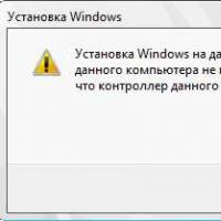 If installing Windows to this disc is not possible
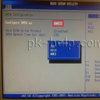 During installation of Windows "Make sure that the controller of this disc is included in the computer's BIOS menu.