Processors. Moving a memory controller directly into modern processors What is an integrated built-in memory controller
It seems that Intel is catching up with AMD in this regard. But, as often happens when the giant does something, then the step is forward to be gigantic. If Barcelona uses two 64-bit DDR2 memory controls, the Topic Intel configuration includes as many three DDR3 memory control. If you install the DDR3-1333 memory that Nehalem also supports, it will give a bandwidth up to 32 GB / s in some configurations. But the advantage of the built-in memory controller lies not only in bandwidth. It significantly reduces the delay in memory access, which is equally important, given that each access costs several hundreds of clocks. In the context of the desktop use, a decrease in the delays in the built-in memory controller can be welcomed, however, the full advantage of the more scalable architecture will be noticeably in multi-sophisticated server configurations. Previously, when adding a CPU, the available bandwidth remained the same, but now each new additional processor increases bandwidth, since each CPU has its own memory.
Of course, no miracles should not be expected. Non Uniform Memory Access (NUMA) configuration, that is, access to memory will be done by one or another optional rates, depending on where the data is located in memory. It is clear that access to local memory will be made with the lowest delays and the highest throughput, since access to the remote memory occurs through the QPI intermediate interface, which reduces performance.
 |
Click on the picture to enlarge.
Impact on performance is difficult because it all depends on the application and the operating system. Intel argues that the performance drop in remote delays is about 70%, and the bandwidth is reduced twice as compared to local access. According to Intel, even with remote access through the QPI interface, the delays will be lower than on previous generations of processors, where the controller was located on the North Bridge. However, this concerns only server applications that have been developed for quite a long time taking into account the NUMA configurations.
Memory hierarchy in CONROE was very simple; Intel concentrated on the performance of the general L2 cache, which became the best solution for the architecture, which was aimed mainly on doubled configurations. But in the case of Nehalem, engineers began from scratch and came to the same conclusion as competitors: the general cache L2 is not very well suited for "native" quad-core architecture. Different kernels may too often "wash" data necessary for other nuclei, which will lead to too many problems with internal tires and arbitration, trying to provide all four kernels with sufficient bandwidth while maintaining delays at a fairly low level. To solve these problems, engineers equipped each kernel with their own cache L2. Since it is highlighted for each core and relatively small (256 KB), it turned out to provide cache with very high productivity; In particular, the delays have improved significantly compared to Penryn - from 15 clocks to, approximately 10 clocks.

Then there is a huge third-level cache (8 MB), which is responsible for the connection between the nuclei. At first glance, the Nehalem cache architecture resembles Barcelona, \u200b\u200bbut the work of the third level cache is very different from AMD - it is inclusive for all the lower levels of the cache hierarchy. This means that if the kernel tries to access data, and they are not available in the L3 cache, then there is no need to look for data in their own caches of other nuclei - there are no them there. On the contrary, if the data is present, four bits associated with each line of cache (one bit on the kernel) are shown whether the data can potentially present (potentially, but without warranty) in the lower cache of another nucleus, and if so, in which.

This technique is very effective to ensure the coherence of the personal caches of each nucleus, since it reduces the need for the exchange of information between the nuclei. There are, of course, the lack of loss of part of the cache memory on the data present in the caches of other levels. However, not everything is so scary, since the L1 and L2 caches are relatively small compared to the L3 cache - all data of cache L1 and L2 occupy a maximum, 1.25 MB in L3 cache from an available 8 MB. As in the case of Barcelona, \u200b\u200bthe third-level cache works at other frequencies compared to the chip itself. Consequently, the delay of access at this level may vary, but it should be about 40 clocks.
The only disappointments in the new hierarchy of NEHALEM cache are associated with L1 cache. The capacity of the cache instruction was not increased - still 16 bytes on the tact compared to 32 at Barcelona. This can create a "bottleneck" in a server-oriented architecture, since 64-bit instructions are larger than 32-bit, especially since Nehalem has one decoder more than Barcelona, \u200b\u200bwhich is stronger than cache. As for the data cache, its delay has been increased to four clocks compared with three CONROE, facilitating the work at high clock frequencies. But we will finish on positive news: Intel engineers increased the number of L1 data cache misses, which architecture can handle in parallel.
TLB.
For many years, processors have been working not with physical memory addresses, but with virtual. Among other advantages, this approach allows you to allocate the program more memory than in the computer, while maintaining only the data you need in physical memory, and everything else is on the hard disk. This means that each memory access is a virtual address to be translated into the physical address, and to save conformity you have to use a huge table. The problem is that this table is so far so far that it cannot be stored on it - it is posted in the main memory, and you can even drop it onto a hard disk (part of the table may be absent in memory, being discarded on HDD).
If there would be a step of translation of addresses for each memory operation operation, then everything would work too slowly. Therefore, engineers returned to the principle of physical addressing, adding a small cache memory directly to the processor that stores compliance for several recently requested addresses. Cache memory is called Translation Lookaside Buffer (TLB). Intel completely redested the TLB in the new architecture. Until now, Core 2 has used the TLB of the first level of very small size (16 records), but very fast and only for downloads, as well as a large second-level TLB cache (256 entries), which is responsible for downloads missing in TLB L1, as well as Entries.
Nehalem is now equipped with a full-fledged two-level TLB: the first level TLB cache is divided for data and instructions. Cache TLB L1 for data can store 64 entries for small pages (4K) or 32 entries for large pages (2m / 4m), and the TLB L1 cache for instructions can store 128 entries for small pages (as in the case of CORE2), as well as Seven for large. The second level consists of a unified cache that can store up to 512 records and works only with small pages. The purpose of such an improvement is to increase the performance of applications that use large data arrays. As in the case of a two-level branch prediction system, we have another certificate of server orientation of architecture.
Let's return to SMT for a while, since this technology also affects the TLB. L1 TLB cache for data and TLB L2 are dynamically distributed between two threads. On the contrary, the L1 TLB cache for instructions is statically distributed for small pages, and highlighted for large pages is completely copied - this is quite understandable, given its small size (seven flow records).
Memory access and preliminary sample
Optimized unwired memory access (UNALIGNED MEMORY ACCESS)
In the Core architecture, access to memory led to a number of performance restrictions. The processor was optimized for access to memory addresses, aligned with 64-byte boundaries, that is, the size of the same stitching of the cache. For non-repeated data, access was not only slow, but also the execution of non-repeated instructions for reading or writing was more invalid than in the case of aligned instructions, regardless of the actual alignment of memory data. The reason was that these instructions led to the generation of several micro-operations on decoders, which reduced bandwidth with these types of instructions. As a result, the compilers avoided generate the instructions of this type, substituting the sequence of instructions that are less superimposed instead.
So, reading from the memory in which the two lines of the cache occurred, slowed down about 12 clocks, compared with 10 clock clocks. Intel engineers optimized a similar type of appeals to be performed faster. Let's start with the fact that there is no longer a drop in performance when using non-repeated read / write instructions in cases where data is aligned in memory. In other cases, Intel also optimized access by reducing the performance drop in comparison with the Core architecture.
More pre-sample blocks with more efficient work
In the Architecture of CONROE Intel was especially proud of prediction hardware blocks. As you know, the prediction unit is a mechanism that follows the character of access to memory and tries to predict what data will be required through several clocks. The goal is to preempt to load data to the cache, where they will be located closer to the processor, and at the same time the maximum use of available bandwidth when it is not needed.
This technology gives wonderful results with most desktop applications, but in the server environment it often led to a loss of performance. There are several reasons for such inefficiency. First, access to memory is often more difficult to predict in server applications. Access to the database, for example, is not a linear - if any data item is requested in the memory, this does not mean that the next element will be next. This limits the effectiveness of the preliminary sampling unit. But the main problem was the bandwidth of memory in multi-commocate configurations. As we said earlier, it was already a "bottleneck" for several processors, but, in addition, the pre-sample blocks led to additional load at this level. If the microprocessor does not access memory, then the pre-sample blocks included, trying to use the bandwidth, by their assumption, free. However, blocks could not know if this bandwidth is needed to another processor. This meant that the pre-sample blocks could "select" through the processor throughput, which was the "bottleneck" in such configurations. To solve this problem, Intel did not find anything better how to disconnect the preliminary sampling blocks in such situations - it is hardly the most optimal solution.
According to Intel, this problem has already been solved, but the company does not give any details about the operation of new preliminary sampling mechanisms. All that the company says: Now you do not need to disable blocks for server configurations. However, even Intel has not changed anything, the advantages of the new memory organization and, as a result, large bandwidth should level the negative impact of the preliminary sample blocks.
Conclusion
CONROE has become a serious foundation for new processors, and Nehalem is built just on it. It uses the same effective architecture, but now it is much more modular and scalable, which should guarantee success in different market segments. We do not say that Nehalem has revolutionized the Core architecture, but the new processor has revolutionized the Intel platform, which has now become worthy of compliance for AMD in design, and intel has successfully bypass a competitor.
 |
Click on the picture to enlarge.
With all the improvements made at this stage (integrated memory controller, QPI), it is not surprising to see that changes in the executive nucleus are not so significant. But the return of Hyper-Threading can be considered serious news, and a number of small optimizations should also provide a noticeable productivity gain compared to Penryn on equal frequencies.
It is quite obvious that the most serious increase will be in those situations where the main "bottleneck" was the RAM. If you have read the entire article, then probably noticed that it was on this area that the Intel engineers paid maximum attention. In addition to adding a built-in memory controller, which, no doubt, will give the greatest increase regarding data access operations, there are many other improvements such as large and small - new cache and TLB architecture, unproved memory access and pre-sample blocks.
Given all theoretical information, we look forward to how improvements will affect real-world applications after the release of a new architecture. We will dedicate to this several articles, so stay with us!
Not so long ago, the processors of the AMD64 family appeared on the market, which are based on a new audit core E. This is a kernel manufactured using a technological process with the production standards of 90 nm, as well as using SOI technologies (Silicon on Insulator) and DSL (DUAL STRESS LINER) ) Found an application immediately in several AMD processor rules. The scope of applying the core of the E revision is very different. It can be found as in the Athlon 64 and Athlon 64 FX processors, where it is indicated by the code names of Venice and San Diego; In dual-core CPUs of the Athlon 64 x2 family, where it is called Toledo or Manchester; And also in the SEMPRON processors, where this core is called Palermo.
Developing and brought to the stage of mass production, AMD seeks not only to increase the utmost clock frequencies of its processors, but also to improving their characteristics. The kernel of revision E was the next stage along the way: with its introduction of the Athlon 64 processors and their derivatives acquired new properties. The most notable improvement was the appearance of SSE3 instructions in AMD processors, which were in the competitor's products since the beginning of the release of CPUs with 90 Nm PRESCOTT core. In addition, the integrated memory controller has been also subject to traditional finishing.
Tests have shown that support for SSE3 commands gives very little. Applications that effectively use these instructions today is extremely small, and the SSE3 character itself is unlikely to qualify for the title of a full-fledged subset of the teams.
Therefore, this time we decided to pay more attention to the changes made to the integrated processor memory controller with the EU audit core. It should be noted that in earlier kernels of your CPU AMD not only increased the performance of the memory controller, but also expanded its compatibility with various combinations of various Memory modules. The audit core, known primarily thanks to the Athlon 64 processors with the code name Winchester, in this plan appeared a kind of line. First, in Winchester processors, compared to predecessors, the performance of the memory controller has slightly increased. Secondly, the processors with the Winchester core have become capable of working with DDR400 SDRAM modules installed immediately into all four DIMM slots on the motherboard. It would seem that the optimum will achieve, however, AMD engineers considered otherwise. AMD processors with a revision core E have an even more advanced memory controller.
Where were the efforts of engineers this time? Naturally, certain optimizations were again made to increase the performance of the memory kitroller. So, processor tests with the Venice core showed their slight superiority over analogs with the Winchester core. In addition, compatibility improved again. AMD processors with a revision core of E steel are capable of functioning normally when installing several memory modules of various organizations and volume, which undoubtedly simplifies the choice of components for further upgrade. Also, the processors are based on a new core, now they can work without any problems with four bilateral DDR400 SDRAM modules. Another interesting property of processors with the audit core was the appearance of new divisors defining the frequency of memory. Thanks to this, new CPUs from AMD are now without any reservations support DDR SDRAM, operating at frequencies exceeding 400 MHz.
advertising
In this material, we will look at some of the features listed above the characteristics of the integrated controller of the nucleus of the Euditz kernel, for, as it seems to us, they clearly deserve.Work with four double-sided DDR400 SDRAM modules
An integrated Athlon 64 processor memory controller is a fairly capricious node. Various unpleasant moments associated with its operation began to figure out from the moment processors appear with the support of two memory channels. It turned out that due to a sufficiently high electrical load, which is imposed by memory modules to the controller, Athlon 64 has certain problems when working with four DIMM modules. So, when installing in the system based on Athlon 64 of the four memory modules, the CPU can reset their frequency, increase the timings or not work at all.
However, the Justice should be noted that the Athlon 64 server analogue, Opteron, such problems devoid through the use of more expensive register modules. However, the use of such modules in desktop systems is unjustified, and therefore users need to put up with some restrictions arising from the installation of more than two DIMM modules.
However, gradually the problems described are still solved. While the old Athlon 64 processors, based on 130 nm technology cores, could not work with four DDR400 SDRAM double-sided modules at a frequency of 400 MHz in general and reduced their frequency to 333 MHz, modern processors with 90 nm nuclei offer users a few Best options. Already in the audit of the D, known to us by the Code name WinChester, it became possible to work with four double-sided DDR400 SDRAM modules, provided that the COMMAND RATE timing is installed in 2t.
Nowadays, in the civilized world, you can hardly find a person who would never have enjoyed the computer and did not have an idea of \u200b\u200bwhat it is. Therefore, instead of once again tell about all the well-known parts of this complex system, we will tell you about something that you still do not know. We will discuss and give a small characteristic of memory controllers, without which the computer work would be impossible. If you want to delve into the system of your personal computer or laptop, then you must know it. And so, let's discuss today, what are memory controllers.
The task that stands before the computer's memory controllers is very important for the computer. The memory controller is a chip that is located on the motherboard or on the central processor. The main function that this tiny chip performs is to manage data flows, both incoming and outgoing. The secondary function of the memory controller is the increase in the potential and performance of the system, as well as uniform and correct placement of information in memory, which is available thanks to new developments in the field of new technologies.
Placing the memory controller in the computer depends on certain models of motherboards and central processors. In some computers, designers placed this chip on the northern parallel accession of the motherboard, while in other computers they are placed on the "DIE" central processor. Those systems that are designed to install a controller in the motherboard have a large number of new different physical nests. RAM, which is used in computers of this type, also have a new modern design.
The main goal of using the memory controller in the computer is that the system can read and write changes in RAM, as well as update it with each download. This is due to the fact that the memory controller sends electrical charges, which in turn are signals for performing certain actions. Do not deepen into technical terminology, we can approve the fact that memory controllers are one of the most important details in a computer that allows you to use the RAM, and without which his work would be impossible.
Memory controllers are of different types. They differ on:
- memory controllers with dual data transfer rate (DDR);
- Completely buffered memory controllers (FB);
- Double controllers (DC).
Functions that can perform memory controllers of different types differ from each other. For example, the memory controllers with a dual data transfer rate are used to transmit data, depending on the increase or decrease in the tempo of the memory hours. While two memory controllers are used in two-channel memory in parallel from each other. This allows the computer to increase the speed of the system, creating more channels, but, despite the difficulties that arise as a result of using a heap of wires, this system works quite efficiently. However, difficulties arise when creating new channels, therefore this type of memory controller is not flawless.
Completely buffered memory controllers from the other side differ from the other types of memory controllers. This technology uses serial data transmission channels that are needed to communicate with the motherboard and unlike the remaining RAM RAM circuits. The advantage of this type of controller is that completely buffered memory controllers reduce the number of wires that are used in the motherboard, and which allows to reduce the time spent on the execution of the task.
As you have already seen, memory controllers are very necessary for stable computer work, and different types are used for different purposes. Prices on the memory range vary from very high to very low, which depends on the type and functions that one or another memory controller performs.
Memory
Memory is a device for storing information. It consists of operational and permanent storage devices. The operational storage device is called Oz, constant storage device - ROM.
RAM- Energy-dependent memory
RAM is intended for recording, reading and storing programs (system and applied), source data, intermediate and final results. Access to the memory elements direct. Other name - RAM Random Access Memory) memory with arbitrary access. All memory cells are combined into groups of 8 bits (1 bytes) and each such group has the address by which you can contact it. RAM is used to temporarily storing data and programs. When the computer is turned off, the information in the RAM is erased. RAM - Energy-dependent memory. In modern computers, the amount of memory is usually from 512 MB to 4 gigabytes. Modern application programs often require 128-256 for their fulfillment, or even 512 MB of memory, otherwise the program simply will not be able to work.
RAM can be built on dynamic chips (Dinamic Random Access Memory - Dram.) or static (Static Random Access Memory - Sram.) type. The static memory type has significantly higher speed, but much more expensive than dynamic. SRAM is used for register memory (MPP and Cash memory), and the main memory RAM is based on the DRAM chip.
ROM is non-volatile memory.
In the English-language literature, the ROM is called Read Only Memory, ROM (read only memory). Information in the ROM is recorded at the memory chip factory, and in the future it is impossible to change its value. The ROM stores information that does not depend on the operating system.
The ROM is:
Processor management program
Display Management Programs, Keyboard, Printer, External Memory
Startup and Stop Programs (BIOS - Base Input / Outout Sysytem)
Programs testing devices that check each time the computer is turned on correct operation of its blocks (Post -Power on SelfTest)
Information about where on the disk is located operating system.
CMOS - non-volatile memory
CMOS RAM is non-volatile computer memory. This multiple chip has a high density of the placement of elements (each cell has a size of 1 byte) and low power consumption - for it quite enough power battery. Computer. Got a name from the technology of creation based on complementary metal-oxide semiconductors ( complemenient Metal-Oxide Semiconductor - CMOS). CMOS RAM is a database for storing a PC configuration information. The SETUP BIOS computer start program is used to install and store configuration settings in CMOS RAM. Each system loading to determine its configuration, the parameters stored in the CMOS RAM microcircuit are read. Moreover, since some computer start parameters can be changed, all these variations are stored in CMOS. The BIOS Setup Installation Program, when recording, saves its system information in it, which is subsequently read (when the PC is loaded). Despite the explicit link between the BIOS and CMOS RAM, these are absolutely different components.
Keywords of this lecture
controllers, Chipset, Ports, USB, COM, LPT, BIOS POST, CMOS, BOOT, C / B Devices,
(controller - Controller, control unit) - a device for managing a variety of computer devices.
Chipset (chipset)
A set of microcircuits designed to collaborate in order to perform a set of any functions. Thus, in computers, the chipset placed on the motherboard performs the role of a binder component that provides the joint functioning of the memory subsystems, the central processor (CPU), I / O and Others. Motherboard (mOTHERBOARD, MB.Also used title mainboard. - main board; slang. mum, mother, motherland) - This is a complex multi-layer printed circuit board, which establishes the main components of the personal computer (the central processor, the RAM controller and the actual RAM, the boot ROM, the controllers of the basic I / O interfaces), chipsets, connectors (slots) to connect additional controllers using USB tires , PCI and PCI-Express.
North Most (NorthBridge; In individual Intel chipsets, Memory Controller Hub, Mch) memory controller system controller chipset on the motherboardthe X86 platforms to which within the organization of the interaction is connected:
through Front Side Bus - microprocessor,
through the memory controller bus - rAM,
through the graphics controller bus - video adapter,
through the inner bus is connected south Most.
South Most (SouthBridge; Function controller; I / O Controller Hub, ICH I / O Controller. Usually this one microcircuit On the motherboard, which through the northern bridge connects with the central processor "Slow" (compared to the "CPU-RAM") interaction (for example, tire connectors for connecting peripheral devices).
AGP. (From English ACCELATED Graphics Port, an accelerated graphic port) - developed in 1997 by Intel, a specialized 32-bit system tire for a video card.
PCI (English Peripheral Component InterConnect, literally - interconnection of peripheral components) - Input / output bus to connect peripheral devices to the computer motherboard.
Ultra DMA (Direct Memory Access, direct memory access). Different versions of ATA are known under the synonyms IDE, EIDE, UDMA, ATAPI; ATA (eng. Advanced Technology Attachment - Adjustment on advanced technology) - a parallel interface for connecting drives (hard drives and optical drives) to a computer. In the 1990s, IBM PC was standard on the IBM PC platform; Currently, it is crowded with its follower - SATA and with his appearance received the name PATA (Parallel ATA).
USB (Eng. Universal Serial Bus - "Universal Serial Tire", pronounced Yu-Es-bi or U-ES-BE) - serial data transmission interface for medium-speed and low-speed peripheral devices in computing technology. To connect the peripheral devices to the USB bus, a four-wire cable is used, and two wires (twisted pairs) are used in differential turn on for receiving and data transmission, and two wires - to power the peripheral device. Thanks to the built-in USB power lines, it allows you to connect peripherals without your own power source (the maximum current power consumed by the USB bus lines should not exceed 500 mA).
LPT.-Port (standard device of the LPT1 Printer Line Printer Terminal or Line Printer) in the MS-DOS family operating systems. IEEE 1284 (printer port, parallel port)
Com.COMMUNICATION PORT, SERIAL PORT, serial port, serial port) - bidirectional serial interface designed to exchange bit information. This port is called this port because information is transmitted through it one bit, bit beyond bit (unlike parallel port).
PS / 2. - The connector used to connect the keyboard and mouse. For the first time appeared in 1987 on IBM PS / 2 computers and subsequently received recognition of other manufacturers and widespread in personal computers and servers of working groups. IBM personal computers series on Intel 80286 and Intel 80386 series processors, manufactured from April 1987. / 2 - version of the computer.
The memory controller is now an integral component of the processor itself. In the AMD processors, the integrated memory controller has been used for more than six years (before the appearance of the architecture of Sandy Bridge), so those who have already been interested in this question, a sufficient amount of information has time to accumulate. However, for Intel processors, occupying a much larger market share (and, therefore, for most users), a change in the nature of the memory system was relevant only together with the output of the company's really mass processors with an integrated memory controller.
Moving the memory controller directly into modern processors strongly affects the overall performance of computer systems. The main factor here is the disappearance of the "mediator" between the processor and memory in the face of the "Northern Bridge". The processor performance no longer depends on the chipset used and, as a rule, in general from the motherboard (that is, the latter turns simply into the backbone).
Next generation RAM, DDR4 SDRAM, brought a significant increase in productivity to server, desktop and mobile platforms. But the achievement of new running speeds requires radical changes in the topology of the memory subsystem. The effective frequency of the DDR4 SDRAM modules will be from 2133 to 4266 MHz. Promising memory modules not only faster, but also more economical than their predecessors. They use reduced to 1.1-1.2 to the supply voltage, and for energy-efficient memory, the voltage is 1.05 V. Manufacturers of DRAM chips in the manufacture of DDR4 SDRAM chips had to resort to the use of the most advanced production technologies.
The mass transition to the use of DDR4 SDRAM was planned for 2015, but it should be borne in mind that the extremely high speeds of memory of the new generation demanded changes to the usual structure of the entire memory subsystem. The fact is that DDR4 SDRAM controllers will be able to cope only with the only module in each channel. This means that a clearly expressed point-to-point topology will come to replace the parallel connection of the memory modules in each channel (each installed DDR4 plan4 will use different channels). To guarantee high frequencies, the DDR4 specification supports only one module to each memory controller. This means that the manufacturers needed to increase the density of memory chips and create more advanced modules. At the same time, the timings continued to grow, although the access time continued to decline.
Samsung Electronics has mastered the release of multi-tiered 512-Mbps DRAM chips using TSV technology. It is this technology that plans to use for the release of DDR4. Thus, it is planned to achieve the issue of relatively low-cost DDR4 memory chips of very high capacity.
Another well known and already proven way to use the so-called "unloading memory" technique - LR-DIMM (Load-Reduce Dimm). The essence of the idea is that the LR-DIMM memory module includes a special chip (or several chips), buffering all tire signals and allowing to increase the number of supported memory system. True, you should not forget about the only one, perhaps, but from this no less significant lack of LR-DIMM: buffering inevitably leads to an additional increase in latency, which in the memory of DDR4 by definition will be without it. For the segment of server and high-end calculations, where a very large amount of memory is in demand, is offered a completely different way out of the situation. It is supposed to use high-speed switching by special multi-voltage switches.
Intel and Micron co-efforts have created a new type of data storage system thatone thousand times faster than the advanced Nand Flash memory. A new type of memory, called 3D Xpoint, shows reading and writing speeds a thousand times higher than the speed of normal NAND memory, and also has a high degree of strength and density. The Cnet news agency reports that the new memory is ten times more denser Nand chips and allows you to save more data on the same physical area and consumes less nutrition. Intel and Micron declare that their new type of memory can be used both as a system and as highly dependent memory, that is, in other words, it can be used as a replacement for both operational RAM memory and SSD. At the moment, computers can interact with a new type of memory via the PCI Express interface, however, Intel says that this type of connection will not be able to reveal the entire potential of the speeds of new memory, therefore, for maximum XPoint memory efficiency, you will have to develop a new motherboard architecture.
Thanks to the new 3DXPOnt technology (cross-point), the memory cell changes the resistance to distinguish between zero and unit. Since the Optane memory cell does not win the transistor, the data storage density in the OPTANE memory exceeds 10 times Nand Flash. Access to an individual cell provides a combination of certain stresses on intersecting conductor lines. The abbreviation is introduced as the cells in memory are located in several layers.
Already in 2017, the technology was widely used and will be used both in the counterparts of flash cards and in RAM modules. Thanks to the new technomalia, computer games will receive a powerful development, because complex locations and cards will be loaded instantly. Intel declares 1000-fold superiority of a new type of memory, compared with the usual flash cards and hard drives. Devices under the Optane brand will produce MICRON using the 20-nm technical process. First of all, a 2.5-inch SSD solid-state drives will be produced, but SSDs will also be released with other sizes, an additionally will be released by the DDR4 operational memory modules for the Intel server platforms.
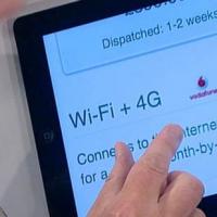 Cellular - what it is on the iPad and what's the difference
 Go to digital television: What to do and how to prepare?
 Social polls work on the Internet
 Savin recorded a video message to the Tyuments
 Menu of Soviet tables What was the name of Thursday in Soviet canteens
 How to make in the "Word" list alphabetically: useful tips
 How to see classmates who retired from friends?