Basic timers in STM32. Working with simple timers STM32 F4 discovery Stm32 timer interrupts
The article describes the timers of 32-bit ARM microcontrollers of the STM32 series from STMicroelectronics. The architecture and composition of the basic timer registers are considered, and practical examples of programs are given.
For any microcontroller, the timer is one of the most important components, which allows you to very accurately count time intervals, count pulses arriving at the inputs, generate internal interrupts, generate signals with pulse width modulation (PWM) and support direct memory access (DMA) processes.
The STM32 microcontroller contains several types of timers that differ from each other in functionality. The first type of timers is the simplest and is Basic Timers. Timers TIM6 and TIM7 belong to this type. These timers are very easy to configure and control using a minimum of registers. They are capable of counting time intervals and generating interrupts when the timer reaches a specified value.
The second type is General-Purpose Timers. This includes timers TIM2 to TIM5 and timers TIM12 to TIM17. They can generate PWM, count pulses arriving at certain pins of the microcontroller, process signals from the encoder, etc.
The third type defines timers with advanced control (Advanced-Control Timer). This type includes the TIM1 timer, which is capable of performing all of the above operations. In addition, based on this timer, you can build a device capable of controlling a three-phase electric drive.
Basic timer device
Let's consider the design and operation of a basic timer, the block diagram of which is shown in the figure. The basic timer is built on the basis of 16-bit registers. Its basis is the counting register TIMx_CNT. (Hereinafter, the symbol “x” replaces the number 6 or 7 for the basic timers TIM6 and TIM7, respectively.) The TIMx_PSC prescaler allows you to adjust the clock frequency for the counter register, and the TIMx_ARR autoload register makes it possible to set the timer counting range . The trigger and synchronization controller, together with the control and status registers, serve to organize the operating mode of the timer and allow you to control its operation.
Thanks to its organization, the timer counter can count forward and backward, as well as to the middle of a given range in the forward direction and then in the reverse direction. The base timer input can be supplied from several sources, including the clock signal from the APB1 bus, an external signal, or the output of other timers applied to the capture and compare pins. Timers TIM6 and TIM7 are clocked from the APB1 bus. If you use an 8 MHz crystal and factory default clock settings, the clock frequency from the APB1 clock bus will be 24 MHz.
Basic Timer Registers
The table shows the register map for the basic timers TIM6 and TIM7. Basic timers include the following 8 registers:
●● TIMx_CNT – Counter (counting register);
●● TIMx_PSC – Prescaler (prescaler);
●● TIMx_ARR – Auto Reload Register;
●● TIMx_CR1 – Control Register 1 (control register 1);
●● TIMx_CR2 – Control Register 2 (control register 2);
●● TIMx_DIER – DMA Interrupt Enable Register (DAP and interrupt enable register);
●● TIMx_SR – Status Register;
●● TIMx_EGR – Event Generation Register.
The TIMx_CNT, TIMx_PSC and TIMx_ARR registers use 16 information bits and allow you to write values from 0 to 65535. The frequency of clock pulses for the TIMx_CNT counter register, passing through the TIMx_PSC divider, is calculated using the formula: Fcnt = Fin/(PSC + 1), where Fcnt is the pulse frequency of the timer counter register; Fin – clock frequency; PSC – contents of the timer TIMx_PSC register, which determines the division coefficient. If you write the value 23999 to the TIMx_PSC register, then the TIMx_CNT counter register at a clock frequency of 24 MHz will change its value 1000 times per second. The automatic loading register stores the value for loading the TIMx_CNT counter register. The contents of the TIMx_CNT register are updated after it is overflowed or reset, depending on the counting direction specified for it. The TIMх_CR1 control register has several control bits. The ARPE bit enables and disables buffering of writes to the TIMx_ARR autoload register. If this bit is zero, then when a new value is written to TIMx_ARR, it will be loaded into it immediately. If the ARPE bit is equal to one, then loading into the register will occur after the event of the counting register reaching the limit value. The OPM discharge enables the “single pulse” mode. If it is set, after the counter register overflows, the counting stops and the CEN bit is reset. The UDIS bit enables or disables the generation of a timer event. If it is cleared, the event will be generated when the event generation condition occurs, that is, when the timer overflows or when the UG bit is programmed in the TIMx_ EGR register. The CEN bit turns the timer on and off. If you reset this bit, the counting will be stopped, and when it is set, the counting will continue. The input divider will start counting from zero. The TIMx_CR2 control register has three control bits MMS2... MMS0, which determine the master mode for the timer. The TIMx_DIER register uses two bits. The UDE bit allows or disables issuing a DMA request when an event occurs. The UIE bit enables and disables timer interrupts. The TIMx_SR register uses only one UIF bit as an interrupt flag. It is installed by hardware when a timer event occurs. You need to reset it programmatically. The TIMx_EGR register contains a UG bit, which allows you to programmatically generate the “counting register overflow” event. When this bit is set, an event is generated and the counting register and prescaler are reset. This bit is reset by hardware. Thanks to this bit, you can programmatically generate an event from a timer, and thereby forcefully call the timer interrupt handler function.
Let's look at the purpose of control registers and timer status using specific program examples.
Example programs
To start a timer, several operations must be performed, such as clocking the timer and initializing its registers. Let's look at these operations using examples of programs for working with timers. Quite often in the programming process the task of implementing time delays arises. To solve this problem, a delay generation function is needed. An example of such a function based on the basic TIM7 timer for STM32 is shown in Listing 1.
Listing 1
#define FAPB1 24000000 // APB1 bus clock frequency // Delay function in milliseconds and microseconds void delay(unsigned char t, unsigned int n)( // Load the PSC prescaler register If(t = = 0) TIM7->PSC = FAPB1 /1000000-1; // for counting microseconds If(t = = 1) TIM7->PSC = FAPB1/1000-1; // for counting milliseconds TIM7->ARR = n; // Load the number of samples into the autoload register ARR TIM7 ->EGR |= TIM_EGR_UG; // Generate an update event // to write data to the PSC and ARR registers TIM7->CR1 |= TIM_CR1_CEN|TIM_CR1_OPM; // Start the timer // by writing the count enable bit CEN // and the mode bit pass OPM to the control register CR1 while (TIM7->CR1&TIM_CR1_CEN != 0); // Waiting for the count to end)
This function can generate delays in microseconds or milliseconds depending on the "t" parameter. The duration of the delay is set by the “n” parameter. This program uses the single pass mode of the TIM7 timer, in which the CNT counter register counts to the overflow value recorded in the ARR register. When these values are equal, the timer will stop. The fact that the timer has stopped is expected in the while loop by checking the CEN bit of the CR1 status register. Enabling clocking of timers is done once in the main module of the program during their initialization. The basic timers are connected to the APB1 bus, so the clock supply looks like this:
RCC->APB1ENR |= RCC_APB1ENR_TIM6EN; // Enable clocking on TIM6 RCC->APB1ENR |= RCC_APB1ENR_ TIM7EN; // Enable clocking on TIM7
The software method for generating a delay described above has a significant drawback due to the fact that the processor is forced to poll the flag throughout the entire delay time and therefore is not able to perform other tasks during this time. This drawback can be eliminated by using the timer interrupt mode. Interrupt handling functions for basic timers typically look like this:
Void TIM7_IRQHandler())( TIM7->SR = ~TIM_SR_UIF; // Clear the flag //Perform operations ) void TIM6_DAC_IRQHandler())( //If the event is from TIM6 if(TIM6->SR & TIM_SR_UIF)( TIM6->SR =~ TIM_SR_UIF ; // Reset the flag // Perform operations ) )
Let's consider an example of a program for organizing a delay on a basic TIM6 timer, which uses interrupts from a timer. To control the execution of the program, we use one of the microcontroller pins to control the LED indicators, which will have to switch at intervals determined by the program delay organized on the TIM6 timer. An example of such a program is shown in Listing 2.
Listing 2
// Including libraries #include
In this program, the delay function is called once, after which the processor can perform other operations, and the timer will regularly generate interrupts at the specified delay interval. A similar program can be written for the TIM7 timer. The difference between such a program will be in the names of the registers and the name of the interrupt handler. The TIM6 timer interrupt handler has one feature related to the fact that the interrupt processing vector for this timer is combined with an interrupt from a digital-to-analog converter (DAC). Therefore, the interrupt handler function checks the source of the interrupt. You can learn more about the timers of the STM32 microcontroller on the St.com website. There are many other tasks for the timer, described above, that it can successfully solve. Therefore, its use in a program significantly lightens the load on the processor and makes the program more efficient.
Any modern controller has timers. This article will talk about simple (basic) timers stm32f4 discovery.
These are ordinary timers. They are 16-bit with automatic reboot. In addition there is a 16-bit programmable frequency divider. It is possible to generate counter overflow interrupts and/or DMA request.
Let's get started. As before I use Eclipse + st-util in ubuntu linux
First of all, we connect the headers:
#include
There is nothing new in this. If it is not clear where they come from, either read previous articles, or open the file and read.
Let's define two constants. One to denote diodes, the other an array of the same diodes:
Const uint16_t LEDS = GPIO_Pin_12 | GPIO_Pin_13 | GPIO_Pin_14 | GPIO_Pin_15; // all diodes const uint16_t LED = (GPIO_Pin_12, GPIO_Pin_13, GPIO_Pin_14, GPIO_Pin_15); // array with diodes
Most likely, you are already familiar with the function of initializing peripherals (that is, diodes):
Void init_leds())( RCC_AHB1PeriphClockCmd(RCC_AHB1Periph_GPIOD, ENABLE); // enable clocking GPIO_InitTypeDef gpio; // structure GPIO_StructInit(&gpio); // fill with standard values gpio.GPIO_OType = GPIO_OType_PP; // pull-up with resistors gpio.GPIO_Mode = GPIO_Mode_OUT; // work as output gpio.GPIO_Pin = LEDS; // all diode pins GPIO_Init(GPIOD, &gpio);
Timer initializer function:
Void init_timer())( RCC_APB1PeriphClockCmd(RCC_APB1Periph_TIM6, ENABLE); // enable timer clocking /* Other parameters of the TIM_TimeBaseInitTypeDef * structure do not make sense for base timers. */ TIM_TimeBaseInitTypeDef base_timer; TIM_TimeBaseStructInit(&base_timer); /* The divisor is taken into account as TIM_Pre scaler + 1, so subtract 1 */ base_timer.TIM_Prescaler = 24000 - 1; // divisor 24000 base_timer.TIM_Period = 1000; //period of 1000 pulses TIM_TimeBaseInit(TIM6, &base_timer); /* Allow interrupt for update (in this case - * for overflow) TIM6 timer counter. */ TIM_ITConfig(TIM6, TIM_IT_Update, ENABLE); TIM_Cmd(TIM6, ENABLE); // Enable the timer /* Enable processing of the TIM6 counter overflow interrupt. * This interrupt is also responsible for emptying the DAC. NVIC_EnableIRQ(TIM6_DAC_IRQn);
I commented the code, so I think everything is clear.
The key parameters here are the divisor (TIM_Prescaler) and the period (TIM_Period) of the timer. These are the parameters that actually configure the operation of the timer.
For example, if you have a clock frequency set to 48 MHz on the STM32F4 DISCOVERY, then the frequency on general-purpose timers is 24 MHz. If you set the divider (TIM_Prescaler) to 24000 (counting frequency = 24MHz/24000 = 1KHz), and the period (TIM_Period) to 1000, then the timer will count the interval in 1s.
Please note that everything depends on the clock speed. You must find out exactly.
I also note that at high frequencies, switching the LED by interruption significantly distorts the frequency value. With a value of 1 MHz at the output I received approximately 250 KHz, i.e. the difference is unacceptable. This result is apparently obtained due to the time spent on executing the interrupt.
Global variable - lit diode flag:
U16 flag = 0;
Interrupt handler that generates the timer. Because The same interrupt is generated when the DAC is running, first we check that it was triggered by the timer:
Void TIM6_DAC_IRQHandler())( /* Since this handler is also called for the DAC, it is necessary to check * whether the TIM6 timer counter overflow interrupt occurred. */ if (TIM_GetITStatus(TIM6, TIM_IT_Update) != RESET) ( flag++; if (flag> 3) flag = 0; /* Clear the bit of the interrupt being processed */ TIM_ClearITPendingBit(TIM6, TIM_IT_Update); GPIO_Write(GPIOD, LED); // light the next diode)
main function:
Int main())( init_leds(); init_timer(); do ( ) while(1); )
We leave the cycle empty. The counter performs its work asynchronously, and the interrupt is an interrupt, so as not to depend on the operation currently being performed.
Good afternoon. Today I’ll write the first article on timers in STM32. In general, the timers in STM32 are so cool that even Schwarzenegger nervously smokes because of the coolness))) And you will have to study them in more than one, or two, or three articles. But first, let’s not bother ourselves too much, but simply study the first simple timers and work with them.
In STM32 there are generally three types of timers
1) basic timers
2) general-purpose timers
3) advanced (advanced-control timers)
Advanced timers are the coolest and combine the capabilities of the two previous groups, plus many additional functions such as working with three-phase motors, etc. and so on. We are still a long way from them, so in this part we will consider working with basic timers.
First, let's look at what timers are on our STM32F407VG processor (you look at your processors with which you work)). My processor has 14 timers - 12 - 16 bit and 2 32 bit
As we see in the pictures, timers TIM2, TIM3, TIM4, TIM5, TIM6, TIM7, TIM12 are connected to the ARV1 bus
And to the ARV2 bus - TIM1, TIM8, TIM9, TIM10, TIM11
Now let's look at the picture of setting up our clocking in the CubeMX program. I will also describe the clocking system separately, since I can’t live without it, but for now I’ll just show how we can clock our timers using the internal HSI clock source.
Here is our standard clock setting without any frequency multipliers, etc. This is what we will use.
And here is an option to speed up the work)) But I advise you not to climb too much with your playful little hands, otherwise it can put the processor on its shoulder blades)) We will study and consider all this later.
So, we open the Reference Manual on the F4 series of microcontrollers, and start smoking the manual. YES, in STM32 not everything is so simple, so comrades, learn English and read the manuals, because without this you will spend a long time looking for what’s what. I used to have a very hard time reading documentation (apparently because the tasks were simple and I had enough of the usual examples from the Internet). Well, now we read... read... read...
Let's continue...
So timers 6 and 7 are basic timers. They sit on the ARV1 bus as we see in the picture from the reference manual.
Basic timers 6 and 7 are 16-bit, have an adjustable prescaler from 0 to 65535. For these timers there are these registers available for reading/writing.
Counter Register (TIMx_CNT) - counter
Prescaler Register (TIMx_PSC) - prescaler
Auto-Reload Register (TIMx_ARR) - reload register
We won’t delve too deeply into the details of the work, since there are 10 pages of descriptions of the registers available to us, etc., the three written above will be enough for us
So, what are these registers and why do we need them? Yes, that's why. We decided to urgently blink an LED, to surprise our fellow AVR-ers, for example, and we say - whoever can quickly set up blinking of one LED with a period of half a second, and the second with a period of a second, wins. (by the way, you can do a similar experiment))))
In order to implement this we need only 5 steps - 1
1) Launch CubeMX and create a project for our controller.
2) in CubeMX set the operation of timers
3) generate a project and open it in Keil uVision
4) initialize timers (one line per timer)
5) write in the interrupt of each timer the code for constantly changing the state of the leg to which the LED is connected.
So let's look at this in more detail. First of all, let's launch our CubeMX program
and configure our 2 pins PD12 and PD13 to output (legs where the LEDs are connected). We set the GPIO_Output mode for them, and the Output Push_Pull mode.
Next on the left we activate our basic timers 6 and 7.
Now go to the configuration tab. As we remember, we did not change anything in the frequency settings for our processor, so we have all buses clocked at -16 MHz. Now, based on this, and based on what we need to get, let's configure our values for the prescalers and the auto-reload register.
As we remember, we need one LED to blink with a frequency of 1 Hz (period 1000 ms), and the second with a frequency of 2 Hz (period 500 ms). How do we get this? It’s very simple. Since any prescaler can be installed on the STM32, we will simply calculate its value
So our frequency is 16,000,000 ticks per second, but we need 1000 ticks per second. This means 16,000,000 \ 1,000 = 16,000. We enter this number minus 1 into the value of the prescaler. That is, the number we get is 15999.
Now our timer is ticking 1000 times per second. Next, we must indicate when we need an overflow interrupt. To do this, we write the number we need in Counter Period (autoreload register).
That is, we need to receive one interrupt per second, and as we remember, our timer ticks 1 time per millisecond. There are 1000 ms in one second, so we enter this value into the auto-reboot register.
In order to get an interruption once every half a second, we write accordingly - 500.
So, we’ve set it up, now we can safely generate our project. Generated, good. There is just a little time left until the LEDs blink.
We opened our project. In principle, everything is set up and ready for us, we just need to start our timers, since even though CubeMX does everything for us, it no longer does this. So, let’s initialize
our timers are with these lines
HAL_TIM_Base_Start_IT(&htim6);
HAL_TIM_Base_Start_IT(&htim7);
This is where our interrupt handlers for our timers are located.
Here is the interrupt handler for timer 7
void TIM7_IRQHandler(void)
{
/* USER CODE BEGIN TIM7_IRQn 0 */
/* USER CODE END TIM7_IRQn 0 */
HAL_TIM_IRQHandler(&htim7);
/* USER CODE BEGIN TIM7_IRQn 1 */
/* USER CODE END TIM7_IRQn 1 */
}
We enter into the interrupt handler what we want to do - and with each interrupt we want to change the state of our legs to which the LEDs are connected.
We use this construction - HAL_GPIO_TogglePin(GPIOD, GPIO_PIN_13);
That's all. We press F7, make sure there are no errors - and we can upload all this stuff to our experimental processor.
Well, we can already enjoy the interesting blinking of the LEDs.
I’ll add a video a little later, but for now, as usual, the picture is correct. Well, don’t forget about gratitude))
Timers in STM32, like all peripherals in principle, are very sophisticated. The abundance of different functions that timers can perform can even make your head spin. Although, it would seem that the timer is just a timer, just to count. But in reality everything is much cooler)
Not only do timers have such wide capabilities, but each controller also has several of them. And not even two or three, but more! In general, one can praise all this endlessly. Let's figure out what and how it works. So, the STM32F103CB microcontroller has:
- 3 general purpose timers (TIM2, TIM3, TIM4)
- 1 more advanced timer with advanced capabilities (TIM1)
- 2 WDT (WatchDog Timer)
- 1 SysTick Timer
Actually, general-purpose timers and the TIM1 timer are not very different from each other, so we will limit ourselves to considering just one timer. By the way, I chose TIM4. No particular reason, I just felt like it =). Timers have 4 independent channels that can be used for:
- Signal Capture
- Comparisons
- PWM generation
- Single pulse generation
- Overflow
- Signal Capture
- Comparison
- Trigger event
When any of these events occurs, timers can generate a request to DMA (DMA is direct memory access, we will deal with that soon =)). Now a little more about each of the timer operating modes.
Signal capture mode. It is very convenient to measure the pulse repetition period when operating the timer in this mode. See for yourself: a pulse arrives, the timer puts its current counter value into the register TIM_CCR. We quickly take this value and hide it in some variable. We sit and wait for the next impulse. Oops! The impulse has arrived, the timer again pushes the counter value into TIM_CCR, and all we have to do is subtract from this value the one that we previously saved. This is probably the simplest use of this timer mode, but very useful. You can catch both the leading edge of a pulse and the trailing edge, so the possibilities are quite large.
Comparison mode. Here we simply connect some timer channel to the corresponding output, and as soon as the timer counts to a certain value (it is in TIM_CCR) the output state will change depending on the mode setting (it will either be set to one, or zero, or change to the opposite).
PWM generation mode. Well, everything is hidden in the name) In this mode, the timer generates PWM! There’s probably no point in writing anything here right now. Soon there will be a sample just for PWM, and we’ll dig into it in more detail.
Dead-Time mode. The essence of the mode is that a certain delay appears between the signals at the main and complementary pins of the timer. There is quite a lot of information on the Internet about where this can and should be applied.
Well, in principle, very briefly about the main operating modes of the timer. If you have questions about other modes, more specific ones, write in the Comments 😉
We need to slowly write a program to work with timers. But first, let's see what's in the Standard Peripheral Library. So, the files are responsible for the timers - stm32f10x_tim.h And stm32f10x_tim.c. We open the first one and see that the file structure repeats the structure of the file for working with GPIO, which we discussed in the previous article. This describes the structures and fields of the structures that are needed to configure timers. True, there is not just one, but several structures (timers have more modes, and therefore settings, than I/O ports). All structure fields are provided with comments, so there shouldn't be any problems here. Well, for example:
| uint16_t TIM_OCMode; // Specifies the TIM mode. |
Here we will set the operating mode of the timer. And here's another:
| uint16_t TIM_Channel; // Specifies the TIM channel. |
Here we select the timer channel, nothing unexpected) In general, everything is quite transparent, if you ask anything =) The first file is clear. And in the file stm32f10x_tim.c– ready-made functions for working with timers. Everything is also generally clear. We have already used the library to work with GPIOs, now we are working with timers, and it is obvious that for different peripherals everything is very similar. So let's create a project and write a program.
So, let's create a new project, add all the necessary files:
We write the code:
It should be noted that in the TIM_Prescaler field you need to write a value that is one less than the one we want to get.
| /****************************timers.c****************** *************/#include "stm32f10x.h" #include "stm32f10x_rcc.h" #include "stm32f10x_gpio.h" #include "stm32f10x_tim.h" //With this prescaler I get one timer tick per 10 µs#define TIMER_PRESCALER 720 /*******************************************************************/ //Variable to store the previous state of the PB0 pin uint16_t previousState; GPIO_InitTypeDef port; TIM_TimeBaseInitTypeDef timer; /*******************************************************************/ void initAll() ( //Enable clocking of the GPIOB port and TIM4 timer //Timer 4 hangs on the APB1 bus RCC_APB2PeriphClockCmd(RCC_APB2Periph_GPIOB, ENABLE) ; RCC_APB1PeriphClockCmd(RCC_APB1Periph_TIM4, ENABLE) ; //Here we configure the PB0 port for output //More about this in the article about GPIO GPIO_StructInit(& port) ; port.GPIO_Mode = GPIO_Mode_Out_PP; port.GPIO_Pin = GPIO_Pin_0; port.GPIO_Speed = GPIO_Speed_2MHz; GPIO_Init(GPIOB, & port) ; //And here is the timer setting //Fill the structure fields with default values TIM_TimeBaseStructInit(& timer) ; //Set the prescaler timer.TIM_Prescaler = TIMER_PRESCALER - 1 ; //Here is the value to which the timer will generate an interrupt //By the way, we will change this value in the interrupt itself timer.TIM_Period = 50 ; //Initialize TIM4 with our values TIM_TimeBaseInit(TIM4, & timer) ; ) /*******************************************************************/ int main() ( __enable_irq() ; initAll() ; //Set up a timer to generate an update (overflow) interrupt TIM_ITConfig(TIM4, TIM_IT_Update, ENABLE) ; //Start the timer TIM_Cmd(TIM4, ENABLE) ; //Enable the corresponding interrupt NVIC_EnableIRQ(TIM4_IRQn) ; while (1) ( //We are endlessly stupid) All useful work is in the interruption __NOP() ; ) ) /*******************************************************************/ //If the output was 0.. timer.TIM_Period = 50 ; TIM_TimeBaseInit(TIM4, & timer) ; //Clear the interrupt bit TIM_ClearITPendingBit(TIM4, TIM_IT_Update) ; ) else ( //Set zero at the output timer.TIM_Period = 250 ; TIM_TimeBaseInit(TIM4, & timer) ; TIM_ClearITPendingBit(TIM4, TIM_IT_Update) ; ) ) |
In this program we look at what was at the output before the interrupt was generated - if it is zero, we set it to one for 0.5 ms. If there was one, set zero to 2.5 ms. Compile and start debugging =)
A small but very important digression... Our example, of course, will work and it will be quite suitable for testing, but still, in “combat” programs you need to monitor the optimality of the code both in terms of its volume and in terms of performance and consumption memory. In this case, there is no point in using the timer structure, and also in calling the TIM_TimeBaseInit() function every time the period changes. It is more correct to change just one value in one register, namely in the TIMx->ARR register (where x is the timer number). In this example, the code is transformed as follows:
| /*******************************************************************/ void TIM4_IRQHandler() ( //If the output was 0.. if (previousState == 0 ) ( //Set one at the output previousState = 1 ; GPIO_SetBits(GPIOB, GPIO_Pin_0) ; //Period is 50 timer ticks, that is 0.5 ms TIM4->ARR = 50 ; ) else ( //Set zero at the output previousState = 0 ; GPIO_ResetBits(GPIOB, GPIO_Pin_0) ; //And the period will now be 250 ticks – 2.5 ms TIM4->ARR = 250 ; ) TIM_ClearITPendingBit(TIM4, TIM_IT_Update) ; ) /****************************End of file****************** **********/ |
So, let's continue, we have another rake on the way) Namely the error:
..\..\..\SPL\src\stm32f10x_tim.c(2870): error: #20: identifier “TIM_CCER_CC4NP” is undefined
Not as scary as it might seem, go to the file stm32f10x.h, find the lines
Now everything is assembled, you can debug it. Turn on the logic analyzer. On the command line we write: la portb&0x01 and see the output:
We got what we wanted) In other words, everything works correctly. In the next article we will dig into the PWM generation mode, stay in touch 😉
Don't miss a good article about timers in general -.
Capture mode is a special operating mode of the timer, the essence of which is as follows: when the logical level changes at a certain pin of the microcontroller, the value of the counting register is written to another register, which is called the capture register.
What is this for?
Using this mode, you can measure the pulse duration or signal period.
The STM32 capture mode has some features:
- ability to choose which front will be active
- ability to change the frequency of the input signal using a prescaler (1,2,4,8)
- each capture channel is equipped with a built-in input filter
- the source of the capture signal can be another timer
- For each channel there are two flags, the first is set if a capture has occurred, the second if a capture has occurred while the first flag is set
Registers are used to configure the capture mode CCMR1(for 1st and 2nd channels) and CCMR2(for 3 and 4), as well as registers CCER, DIER.
Let's take a closer look at the register bit fields CCMR2, responsible for setting up the 4th channel of the timer, this is what we will be setting up in the example. I would also like to note that the same register contains bit fields that are used when setting the timer in comparison mode.
CC4S- determines the direction of operation of the fourth channel (input or output). When setting a channel as an input, it is assigned a capture signal
- 00 - channel works as output
- 01 - channel works as input, capture signal - TI4
- 10 - channel works as input, capture signal - TI3
- 11 - channel works as input, capture signal - TRC
- 00 - the divider is not used, the IC1PS capture signal is generated for each event
- 01 - a capture signal is generated for every second event
- 10 - a capture signal is generated for every fourth event
- 11 - a capture signal is generated for every eighth event

Now let's look at the register CCER.
CC4E- turns on/off capture mode.
CC4P- determines the front along which the capture will be carried out, 0 - front, 1 - back.
And register DIER.
CC4DE- allows you to generate a request to DMA.
CC4IE- allows capture interruption.
After a capture has occurred, a capture event is generated that sets the corresponding flag. This may result in an interrupt being generated and a request DMA, if they are allowed in the register DIER. In addition, a capture event can be generated programmatically by setting a bit field in the event generation register EGR:
Bit fields CC1G, CC2G, CC3G and CC4G allow you to generate an event in the corresponding capture/comparison channel.
By the way, CCR1, CCR2, CCR3 and CCR4- capture registers, in which the timer value is stored based on the capture signal.
In order to control the generation of the capture signal, in the register S.R. Two flags are allocated for each channel.
CC4IF- set when a capture signal is generated, these flags are reset by software or by reading the corresponding capture/compare register.
CC4OF- set if the CC4IF flag has not been cleared, but another capture signal has arrived. This flag is cleared programmatically by writing zero.
Now let's put this knowledge into practice; from the signal generator we will supply a sinusoid with a frequency of 50 Hz from the signal generator to the TIM5_CH4 input and try to measure its period. In order to speed up the process, I suggest using DMA. Which MK pin corresponds to channel 4 TIM5 can be found in the datasheet on the MK in the section Pinouts and pin description.

For DMA register address required CCR4, here's how to find it. Opening RM0008 and in the table Register boundary addresses find the starting address of TIM5.

offset for register CCR4 can be found in the same document in the section register map.
#include "stm32f10x.h" #define TIM5_CCR4_Address ((u32)0x40000C00+0x40) #define DMA_BUFF_SIZE 2 uint16_t buff;//Buffer uint16_t volatile T; void DMA2_Channel1_IRQHandler (void) ( T = (buff > buff) ? (buff - buff) : (65535+ buff - buff); DMA2->IFCR |= DMA_IFCR_CGIF1; ) void Init_DMA(void) ( RCC->AHBENR |= RCC_AHBENR_DMA2EN ; //Enable clocking of the first DMA module DMA2_Channel1->CPAR = TIM5_CCR4_Address; //Specify the peripheral address - the ADC conversion result register for regular channels DMA2_Channel1->CMAR = (uint32_t)buff; //Set the memory address - the base address of the array in RAM DMA2_Channel1 ->CCR &= ~DMA_CCR1_DIR; //Indicate the direction of data transfer, from the peripheral to the memory DMA2_Channel1->CNDTR = DMA_BUFF_SIZE; //The number of transferred values DMA2_Channel1->CCR &= ~DMA_CCR1_PINC; //The peripheral address is not incremented after each transfer DMA2_Channel1 -> CCR | = DMCR1_MINC; BIT DMA2_ChanNEL1- >CCR |= DMA_CCR1_PL; //Priority - very high DMA2_Channel1->CCR |= DMA_CCR1_CIRC; //Enable DMA operation in cyclic mode DMA2_Channel1->CCR |= DMA_CCR1_TCIE;//Enable interruption at the end of transmission DMA2_Channel1->CCR |= DMA_CCR1_EN; //Enable the operation of the 1st DMA channel) int main(void) ( Init_DMA(); //enable clocking of port A, alternative functions and timer RCC->APB2ENR |= RCC_APB2ENR_IOPAEN | RCC_APB2ENR_AFIOEN; RCC->APB1ENR |= RCC_APB1ENR_TIM5EN; TIM5 ->PSC = 56000-1;//new frequency 1Khz TIM5->CCMR2 |= TIM_CCMR2_CC4S_0;//select TI4 for TIM5_CH4 TIM5->CCMR2 &= ~(TIM_CCMR2_IC4F | TIM_CCMR2_IC4PSC);//do not filter and do not use a divider TIM5- >CCER &= ~TIM_CCER_CC4P;//select capture on the leading edge TIM5->CCER |= TIM_CCER_CC4E;//turn on the capture mode for the 4th channel TIM5->DIER |= TIM_DIER_CC4DE;//allow to generate a request to DMA //TIM5 ->DIER |= TIM_DIER_CC4IE; //enable capture interrupt TIM5->CR1 |= TIM_CR1_CEN; //enable the counter //NVIC->ISER |= NVIC_ISER_SETENA_18; //TIM5 Interrupt NVIC->ISER |= NVIC_ISER_SETENA_24; Interrupt while(1) ( ) )
 Refilling cartridges in Kazan - Printek® Starter cartridge: properties, purpose and capabilities
 Application for making money vk
 Free graphic editors Programs for creating effects in graphics
 Bitcoin Miner is a virus that hunts for your hardware
 Reasons for accelerated discharge
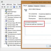 Checking the webcam on a laptop
 How to make an amplifier from a tape recorder